Semiconductor Electronics: Materials,Devices And Simple Circuits - Class 12 Engineering Physics - Extra Questions
What is the energy band gap of:
(i) silicon and (ii) germanium
What is a hole? Which type of doping creats a hole?
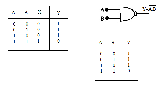
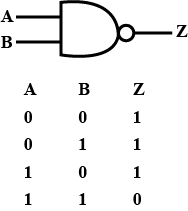
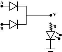
Identify the logic gate whose truth table is given below and draw its symbol:
| $$A$$ | $$B$$ | $$Y$$ |
| $$0$$ | $$0$$ | $$1$$ |
| $$0$$ | $$1$$ | $$1$$ |
| $$1$$ | $$0$$ | $$1$$ |
| $$1$$ | $$1$$ | $$0$$ |
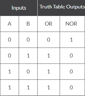
Draw the truth table of a NOR gate.
Which gates are called universal gates?
The use of zener diode is as ________.
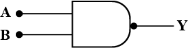
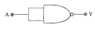
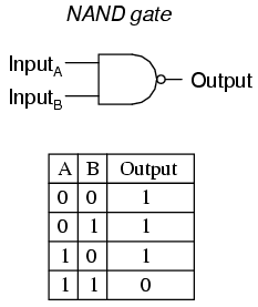
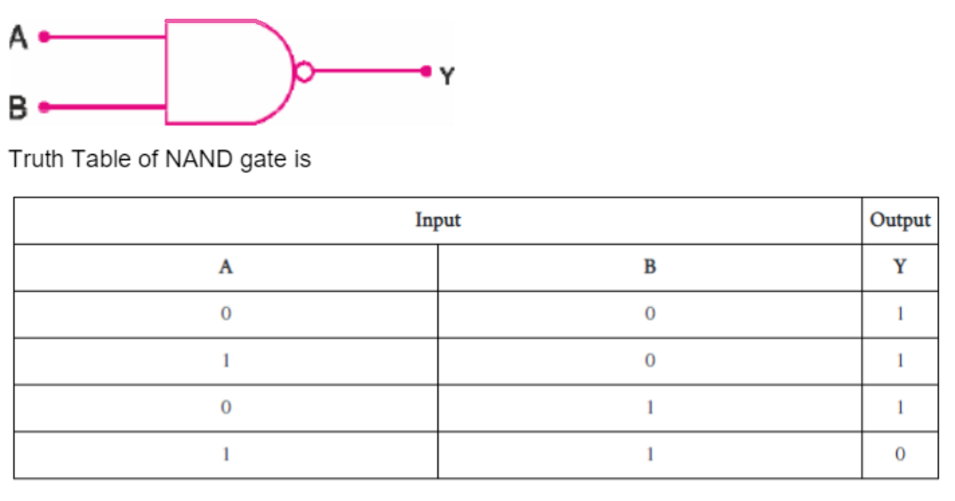
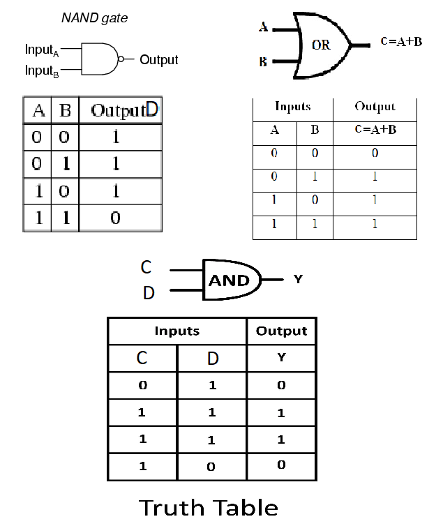
What is a NAND gate? Give its logic symbol.

Write one main use of Zener diode.
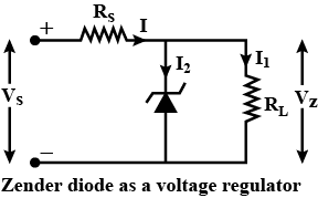
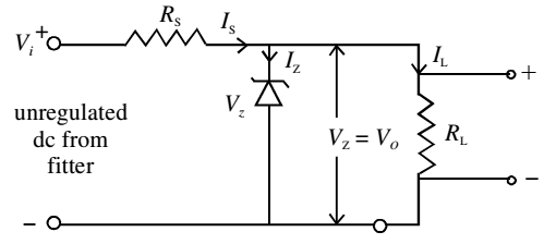
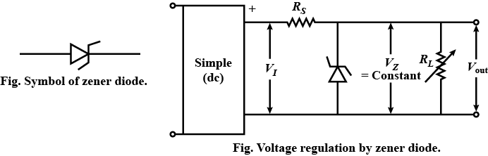
What is Zener diode? How is it used as a voltage regulator?
$$\bullet$$When a Zener diode is biased in the forward direction, it behaves like a conventional signal diode, with current increasing linearly with voltage,
$$\bullet$$When a reverse voltage is applied across the diode and it reaches the device's breakdown voltage, a massive current begins to flow through the diode.

$$\bullet$$Shunt Voltage Regulators like Zener Diodes are commonly used to control voltage across small loads. The reverse breakdown voltage of Zener diodes is acute, and the breakdown voltage remains constant over a wide range of currents.
$$\bullet$$As a result, the zener diode will be connected parallel to the load, causing the applied voltage to reverse bias it. The voltage across the load will remain constant if the reverse bias voltage across the zener diode exceeds the knee voltage.
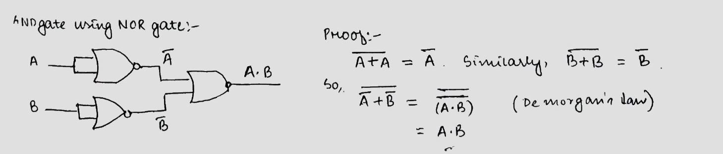
Construct a AND gate using only NOR gates only
A coil a current of $$1.0$$ ampere and a power of $$100$$. Find the Resistance.
Which device is used as a voltage regulator ?
Distinguish between 'paramagnetic' and 'ferromagnetic' substances.
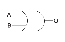
Name the logic gate which generates high output when at least one input is high.
The number of silicon atoms per $$m^3$$ is $$5\, \times\, 10^{28}$$. This is doped simultaneously with $$5\, \times\, 10^{22}$$ atoms per $$m^3$$ of arsenic and $$5 \times\, 10^{20}$$ per $$m^3$$ atoms of indium. Calculate the number of electrons and holes. Given that $$n_i\, =\, 1.5\, \times\, 10^{16}\ /m^{3}$$. Is the material n-type or p-type?
Write the truth table for a NAND gate connected as given in Figure.
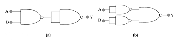
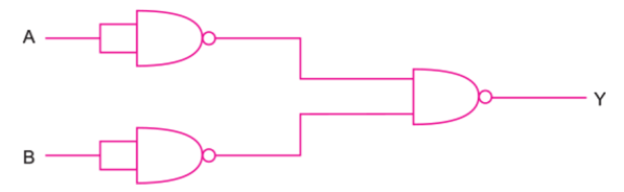
You are given two circuits as shown in Fig., which consist of NAND gates. Identify the logic operation carried out by the two circuits.
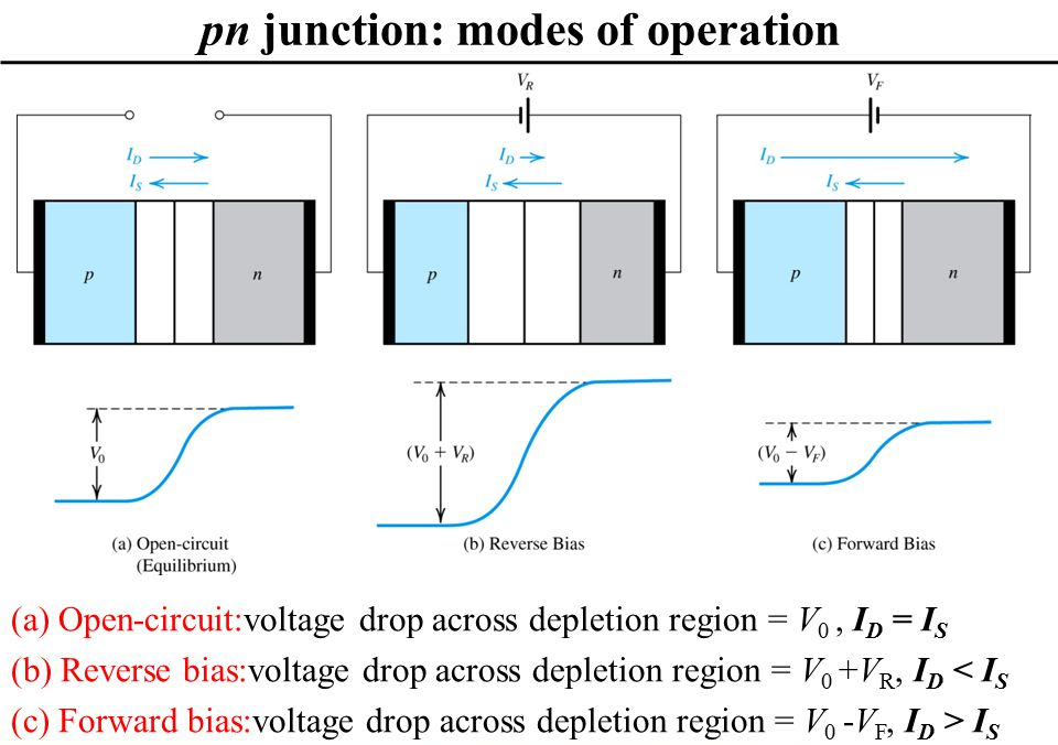
What happens when a forward bias is applied to a p-n junction?
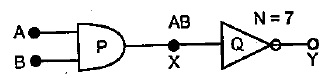
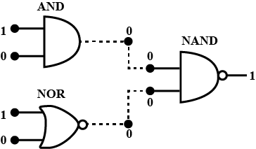
Identify the gates P and Q shown in figure. Write the truth table for the combination of the gates shown.
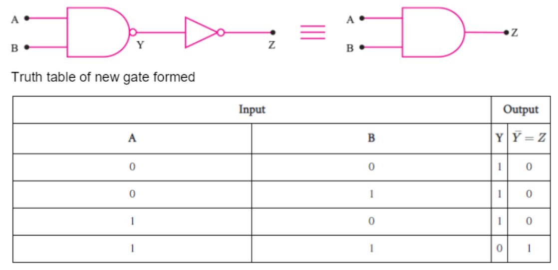
Name of equivalent gate representing this circuit and write its logic symbol
(a) Explain briefly the principle on which a transistor-amplifier works as an oscillator. Draw the necessary circuit diagram and explain its working.
(b) Identify the equivalent gate for the following circuit and write its truth table.
(a) Principle on which a transistor-amplifier works as an oscillator-
The transistor-amplifier oscillatory circuit consists of an inductive coil of inductance L connected in parallel with a capacitor of capacitance C. The frequency of oscillation in the circuit depends upon the values of L and C. The actual frequency of oscillation is the resonant.
The transistor-amplifier oscillatory circuit receives dc power from the battery and converts it into ac power for supply to the circuit. The oscillations occurring in the circuit are applied to the input of the electronic amplifier and due to amplifying properties of the amplifier, we get increased output of these oscillations which can be supplied to the circuit to meet the losses.
( b) The equivalent gate for the following circuit is AND gate and below is its Truth Table

(a) Describe briefly, with the help of a diagram, the role of the two important processes involved in the formation of a $$p-n$$ junction.
(b) Name the device which is used as a voltage regulator. Draw the necessary circuit diagram and explain its working.


How can electrical conductivity of metals, insulator and semiconductors be explained qualitatively?
What is the use of a Zener diode?
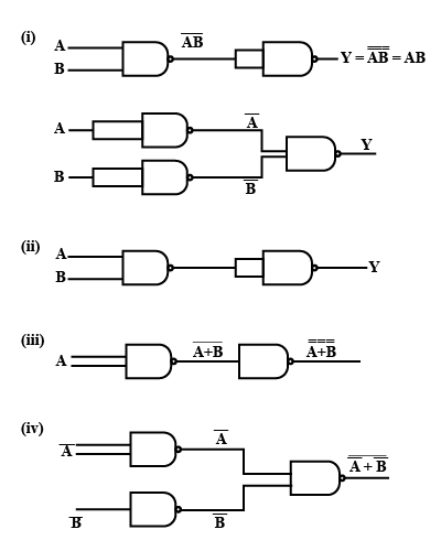
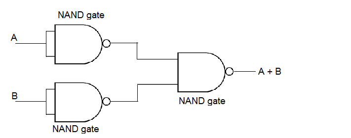
With the help of a diagram, show how you can use several NAND gates to obtain an OR gate.
| A | B | $$\overline A$$ | $$\overline B$$ | Y |
| 0 | 0 | 1 | 1 | 0 |
| 0 | 1 | 1 | 0 | 1 |
| 1 | 0 | 0 | 1 | 1 |
| 1 | 1 | 0 | 0 | 1 |

Write the names of two universal logic gates. What is integrated circuit? Write two advantages of it.
An incandescent lamp is operated at $$240 V$$ and the current is $$0.5A$$. What is the resistance of the lamp?
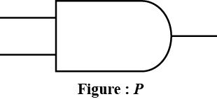
Write the names of logic gates related to figure $$P$$ and table $$Q$$.
Table:$$Q$$
| $$A$$ | $$B$$ | $$Y$$ | $$Y'$$ |
| $$0$$ | $$0$$ | $$0$$ | $$1$$ |
| $$0$$ | $$1$$ | $$1$$ | $$0$$ |
| $$1$$ | $$0$$ | $$1$$ | $$0$$ |
| $$1$$ | $$1$$ | $$1$$ | $$0$$ |
Find the output $$F$$ of the logic circuit given below.

Output of $$2nd$$ OR gate $$= A + C$$
Output of AND gate $$= (A + B).(A + C)$$
$$= AA + BA + AC + BC$$
$$= A(1 + B + C) + BC$$
$$= A(1) + BC$$
$$= A + BC$$

Draw the circuit diagram of a voltage regulator using zener diode.
(a) NAND gates are also called universal gate. Why?
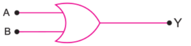
(b) Draw a logic symbol of OR gate.
(c) Write the value of output $$y$$ in the given circuit:
(d) Write the name of the diode used in voltage regulation.
In which bias can a zener diode be used as voltage regulator?
What are universal gates? Why are they called so ?
A light bulb is rated at $$100 W$$ for a $$220 V$$ supply. Find the resistance of the bulb.
Write the logic symbol and truth table of NAND gate.
How will you obtain OR, AND gates from the NAND and NOR gates? Write symbol, Boolean formula and truth table.
For obtaining OR gate from NAND gate the inputs $$A$$ and $$B$$ are connected to the two NOT gates obtained from NAND gates. The input get inverted as $$\overline { A }$$ and $$ \overline { B }$$. These inputs are then fed to the NAND gate as shown in fig. drawn below.
Boolean formual: $$y=\overline { y } =\overline { \overline { A\cdot B } } =A\cdot B$$
| Input | Output |
| A | B | y | y |
| 0 1 0 1 | 0 0 1 1 | 1 1 1 0 | 0 0 0 1 |
Boolean formula: $$ y=\overline { \overline { A } } \overline { \overline { B } } =\overline { \overline { A } } +\overline { \overline { B } } =A+B$$
| Input | Output |
| A 0 1 0 1 | B 0 0 1 1 | $$\overline { A }$$ 1 0 1 0 | $$ \overline { B }$$ 1 1 0 0 | y 0 1 1 1 |
| Input | Output |
| A | $$\overline { A }$$ |
| 0 1 | 1 0 |
Which is inturn are again connected is NOR gate.
Boolean formula: $$ \overline { y } =\overline { A } +\overline { B } =\overline { \overline { A } +\overline { B } } =A\cdot B$$
By using Bolean Algebra prove that $$\bar{A}B + A\bar{B} + AB = A +B$$.
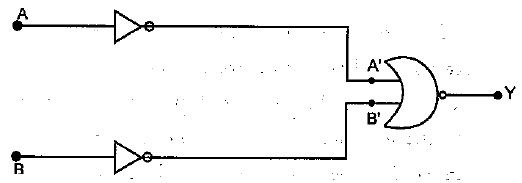
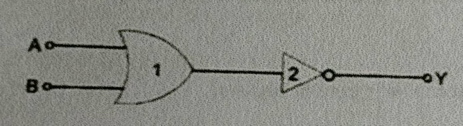
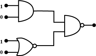
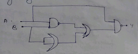
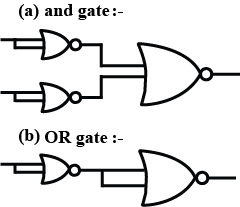
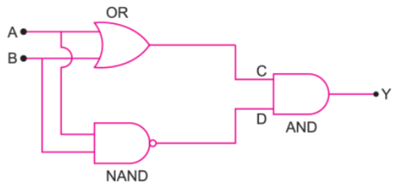
In the given logic circuit, name the logic gates 1 and 2 .
(a) Write the name of the combination of the gates.
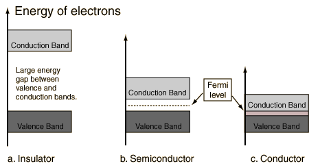
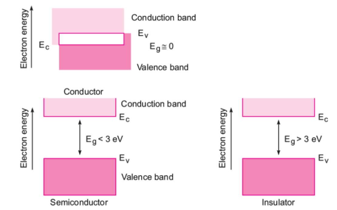
Explain the formation of energy bands in solids. On the basis of energy bands distinguish between a metal, a semiconductor and an insulator.
How is Zener diode used as voltage regulator?
Draw a diagram of show how NAND gates can be combined to obtain an OR gate.(Truth table is not required).
What is optoelectronic junction devices? Write any two names of optoelectronic junction devices.
Draw separate energy band diagrams for conductors, semi-conductors and insulators and label each of them.
In conductors, both the valance band and conduction band overlap each other. So there is zero band gap in a conductor.
In semiconductor, there is a small band gap approximately of $$1 \ eV$$.
In an insulator, there is a large band gap of nearly $$5 \ eV$$.

What is the output of the combination?
$$100\ mg$$ mass of nichrome metal is drawn into a wire of area of cross-section $$0.05{mm}^{2}$$. Calculate the resistance of this wire. Given density of nichrome $$8.4\times {10}^{3}$$ $$kg{m}^{-3}$$ and resistivity of the material as $$\rho =1.2\times { 10 }^{ -6 }\Omega m$$.
If the measured value of resistance $$R = 1.05 \Omega $$ wire diameter $$d = 0.60 mm$$, and length $$l = 75.3 cm$$, then find the maximum permissible error in resistivity, $$\rho = \frac{R(\pi d^2 /4)}{l}$$
Mention practical importance of Zener diode in a laboratory.
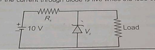
In a zener-regulated power supply a zener diode with $$V_{z}=6 $$ volt is used for regulation. The load current is to be $$4\ mA$$ and the unregulated input is $$10$$ volt. What should be the value of series resistor $$R_{s}$$ if the current through diode is five times the load current?
Find out output for given logic gate:
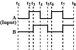
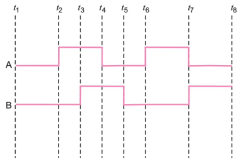
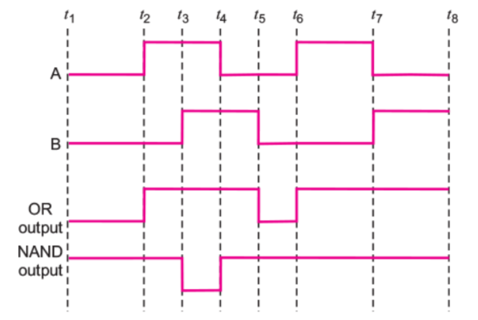
The figure shows the input waveforms A and B for 'AND' gate.
Draw the output waveform and write the truth table for this logic gate.
Three resistors each of $$2 \Omega$$ are connected together so that their total resistance is $$3 \Omega$$. Draw a diagram to show this arrangement and check it by calculation.
What is internal resistance and ideal voltmeter?
Draw energy band diagrams of $$n$$ -type and $$p$$ -type semiconductors at temperature $$\mathrm { T } > 0$$ K. Mark the donor and acceptor energy levels with their energies .
Given the ratio of the numbers of holes and the number of conduction electrons in an intrinsic semiconductor.
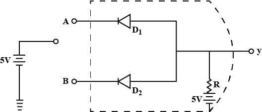
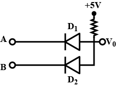
(a) What are logic gates?
(b) Draw a circuit diagram for dual-input AND Gate by using two diodes.
(b) Circuit diagram of AND gate by using two diodes.(Refer...image)
Why are NOR gates considered as universal gates?
Draw the symbol of NAND gate and write down truth table for this. Why is it called a universal gate?
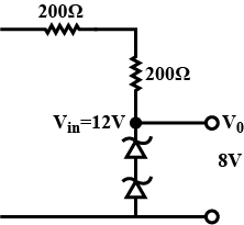
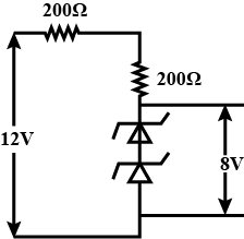
The circuit shown below is working as a $$8\ V\ dc$$ regulated voltage source. When $$12\ V$$ is used as input, the power dissipated (in $$mW$$) in each diode is; (considering both zener dioses are identical)____________
Let $$\Delta \,E$$ denote the energy gap between the valence band and the conduction band. The population of conduction electrons (and of the holes) is roughly proportional to $$e^{-\Delta \, E /2kT}$$. Find the ratio of the concentration of conduction electrons in diamond to that in silicon at a room temperature 300 K. $$\Delta \,E$$ for silicon is $$1\cdot1\, eV$$ and for diamond is $$6\cdot 0\, eV$$.
The output of a $$ 2$$-input AND gate is fed to a NOT gate. Give the name of the combination and its logic symbol. Write down its truth table.
Write the truth table for the logic circuit shown below and identify the logic operation performed by this circuit.
Truth Table
| $$ A $$ | $$ B $$ | $$ Y $$ |
| $$ 0 $$ | $$ 0 $$ | $$ 0 $$ |
| $$ 1 $$ | $$ 0 $$ | $$ 1 $$ |
| $$ 0 $$ | $$ 1 $$ | $$ 1 $$ |
| $$ 1 $$ | $$ 1 $$ | $$ 1 $$ |
Draw the necessary energy band diagrams to distinguish between conductors, semiconductors and insulators. How does the change in temperature affect the behaviour of these materials ? Explain briefly.
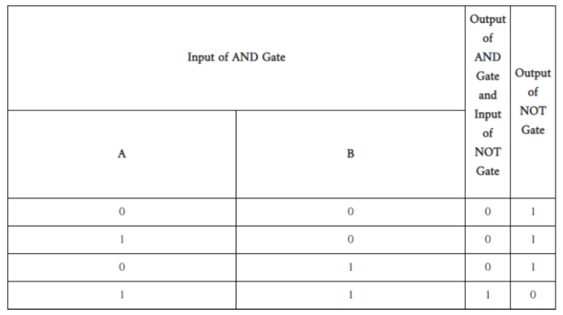
Using truth table of AND gate and NOT gate , show that NAND gate is an AND gate followed by a NOT gate. Hence write the truth table of NAND gate. Why are NAND gates called 'Universal Gates' ?
| $$ A $$ | $$ B $$ | Output of NAND Gate |
| $$ 0 $$ | $$ 0 $$ | $$ 1 $$ |
| $$ 1 $$ | $$ 0 $$ | $$ 1 $$ |
| $$ 0 $$ | $$ 1 $$ | $$ 1 $$ |
| $$ 1 $$ | $$ 1 $$ | $$ 0 $$ |
All primary gates likes AND , NOT and OR gates can be realised by using NAND gate only. Hence , it is a universal gate.
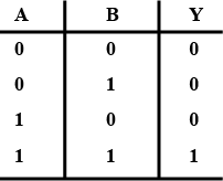
The following table gives the output of a two input logic gate.
If the output of this gate is fed as input to a NOT gate, name the new logic gate so formed.
| $$ A $$ | $$ B $$ | $$ Y $$ |
| $$ 0 $$ | $$ 0 $$ | $$ 1 $$ |
| $$ 1 $$ | $$ 0 $$ | $$ 1 $$ |
| $$ 0 $$ | $$ 1 $$ | $$ 1 $$ |
| $$ 1 $$ | $$ 1 $$ | $$ 0 $$ |
Write the truth table for the circuit shown in figure. Name the gate that the circuit resembles.
Identify the logic gate represented by the following circuit by writing its truth table :
Answer the following questions.
Show the output waveforms (Y) for the following inputs A and B of
(i) OR gate (ii) NAND gate
Why is a Zener diode considered as a special purpose semiconductor diode ?
Draw the I-V characteristics of a Zener diode and explain briefly how reverse current suddenly increases at the breakdown voltage.
Describe briefly with the help of a circuit diagram how a Zener diode works to obtain a constant dc voltage from the unregulated dc output of a rectifier.
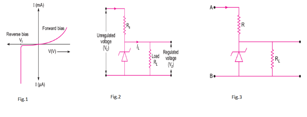
Explain how a Zener diode maintains a constant voltage across a load.
In an intrinsic semiconductor the energy gap $$E_g$$ is $$1.2\ eV$$. Its hole mobility is much smaller than electron mobility and independent of temperature. What is the ratio between conductivity at $$600\ K$$ and that at $$300\ K$$? Assume that the temperature dependence of intrinsic carrier concentration $$n_i$$ is given by
$$n_i = n_o exp \left(- \dfrac{E_g}{2 k_B T} \right)$$
Where $$n_0$$ is a constant.
What happens to the potential barrier of a p-n junction diode when it is?
Draw the circuit diagram of OR-gate using diodes.
Explain the variation of conductivity with temperature for (i) a metallic conductor (ii) Ionic conductors and (iii) semiconductors
Where m=mass of charge carrier,e=charge on each carrier.
T=relaxation time, n=number density of chargecarries.
i)With rise of temperatue, the collision of electrons with fixed lattice ions/atoms increases so that relaxation time (T) decreases.Consequently, the conductivity of metals decreases with rise of temperature.
ii) Conductivity of ionic conductor increases with increase of temperature because with increase of temperature, the ionic bonds break releasing positive and negative ions which are charge carriers in ionic conductors.
iii) In the case of a semiconductors, when temperature increases, covalent bonds break and charge carriers (electrons and holes) becomes free i.e. n increases, so conductivity increases with rise of temperature.
$$Sn,C$$ and $$Si,Ge$$ are all group XIV elements. Yet, $$Sn$$ is a conductor, $$C$$ is an insulator while $$Si$$ and $$Ge$$ are semiconductors. Why?
Draw the circuit used for voltage regulation in a Zener diode and also explain its process in short.
Class 12 Engineering Physics Extra Questions
- Alternating Current Extra Questions
- Atoms Extra Questions
- Current Electricity Extra Questions
- Dual Nature Of Radiation And Matter Extra Questions
- Electric Charges And Fields Extra Questions
- Electromagnetic Induction Extra Questions
- Electromagnetic Waves Extra Questions
- Electrostatic Potential And Capacitance Extra Questions
- Magnetism And Matter Extra Questions
- Moving Charges And Magnetism Extra Questions
- Nuclei Extra Questions
- Ray Optics And Optical Instruments Extra Questions
- Semiconductor Electronics: Materials,Devices And Simple Circuits Extra Questions
- Wave Optics Extra Questions