Semiconductor Electronics: Materials, Devices And Simple Circuits - Class 12 Medical Physics - Extra Questions
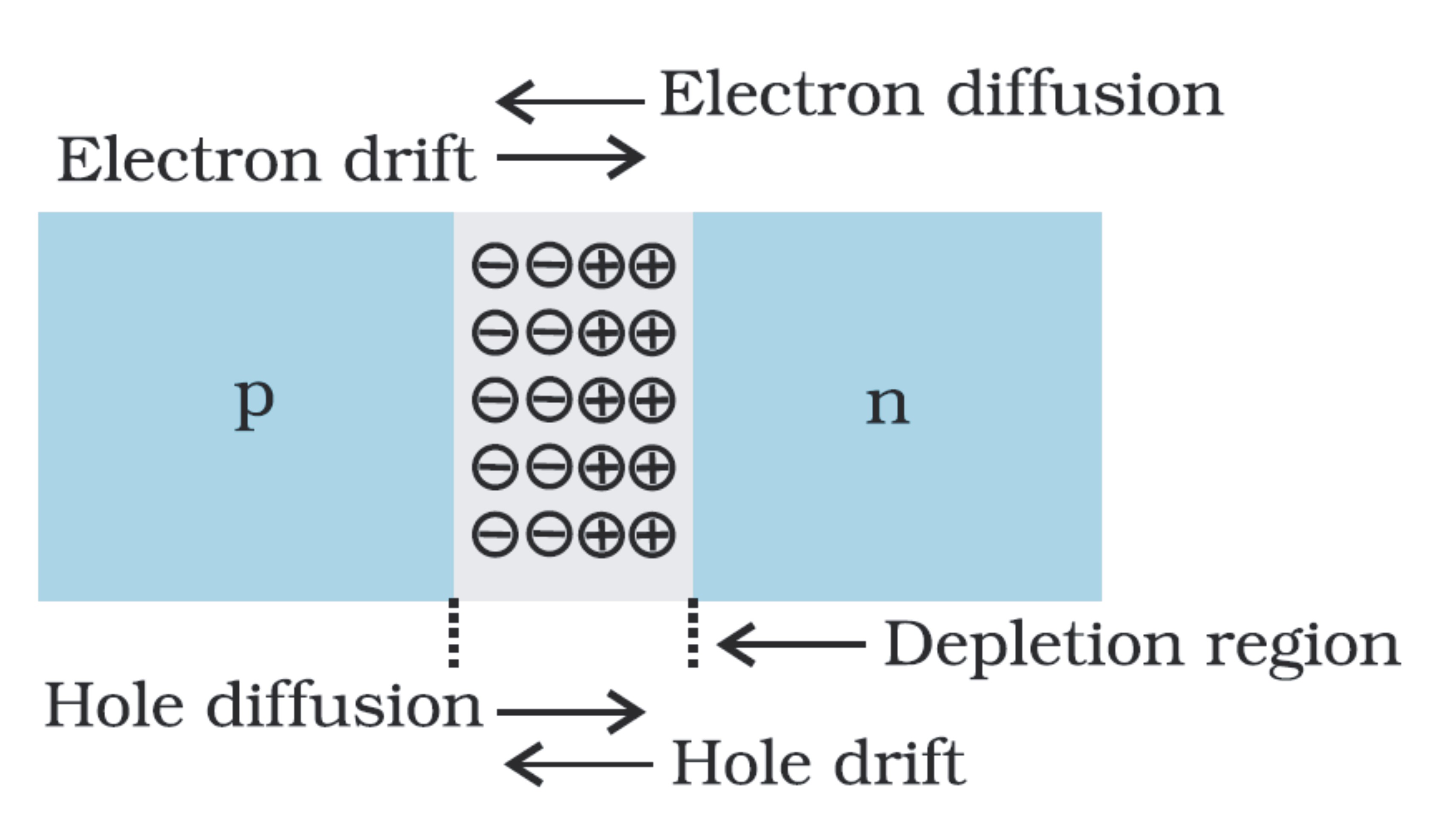
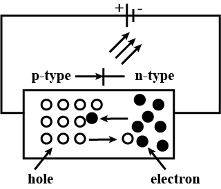
Describe briefly , with the help of a diagram, the role of the two important processes involved in the formation of a pn junction.
Write he name of any one doped semiconductor used for making light emitting diode (LED)
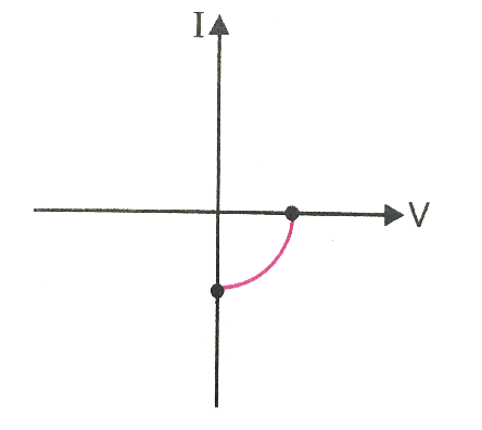
Name the junction diode whose $$I - V$$ characteristics are drawn below :
A Zener diode is fabricated by heavily doping both p- and n- sides of the junction. Explain, why?
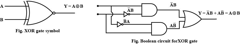
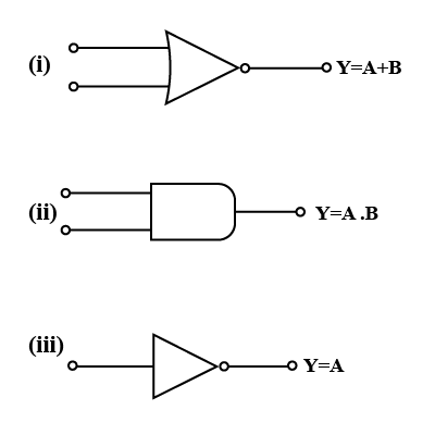
What do you understand by the logic gate? Draw the symbol for XOR gate and also the truth table.
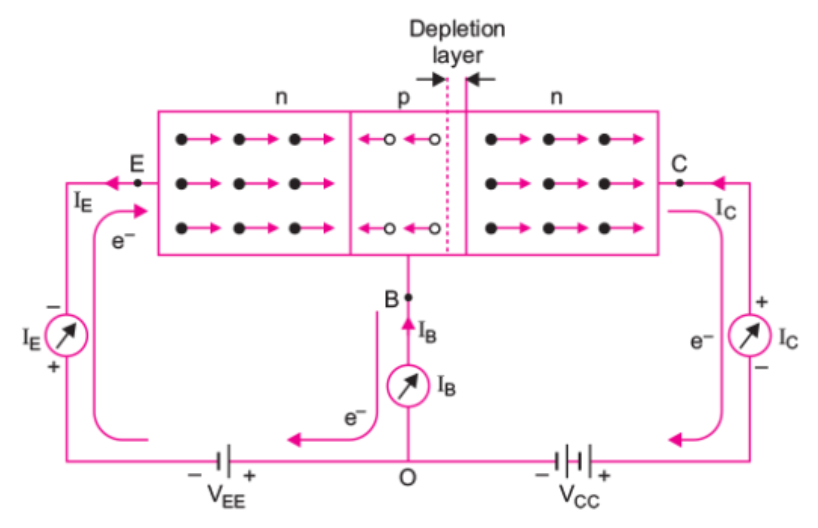
In a transistor why is the base made thin in comparison to the emitter and collector?
Make truth table for OR gate.
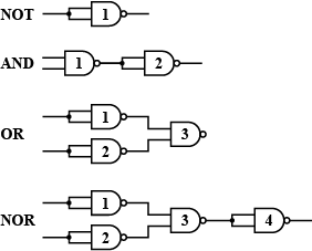
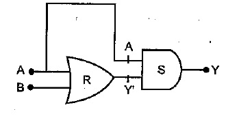
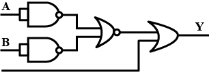
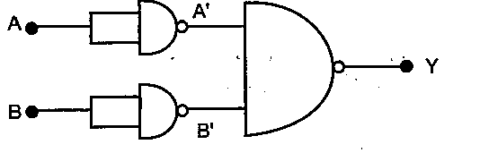
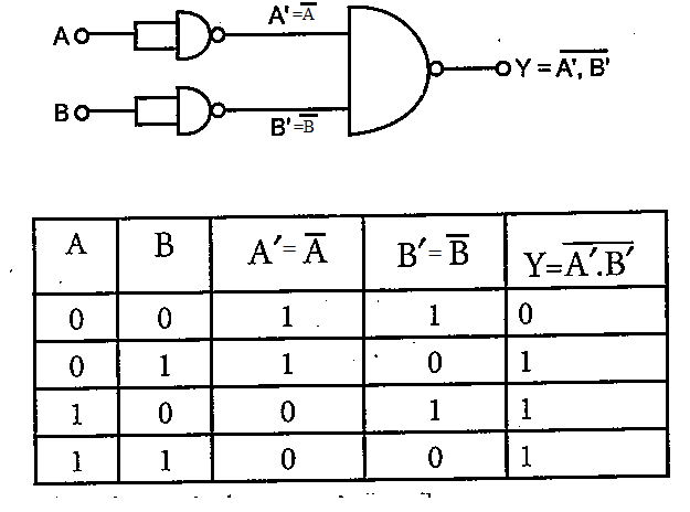
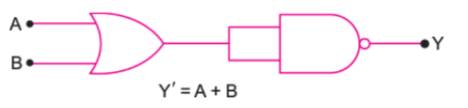
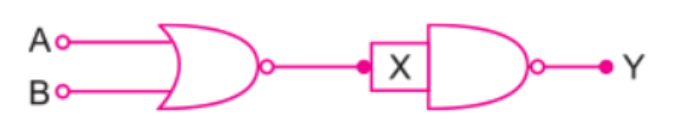
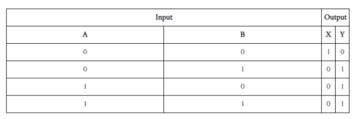
Write the truth table for circuit given in the figure, consisting of NOR gates and identify the logic operation (OR, AND, NOT) which this circuit is performing.
(Hint: A = 0, B = 1 then A and B inputs of second NOR gate will be 0 and hence Y=Similarly work out the values of Y for other combinations of A and B. Compare with the truth table of OR, AND, NOT gates and find the correct one).
$$E_{g}(T)=E_{g}(m)-{\dfrac {\alpha T^{2}}{T+\beta }}$$ is the Varshni's empirical expression,then the value of $$m$$ is
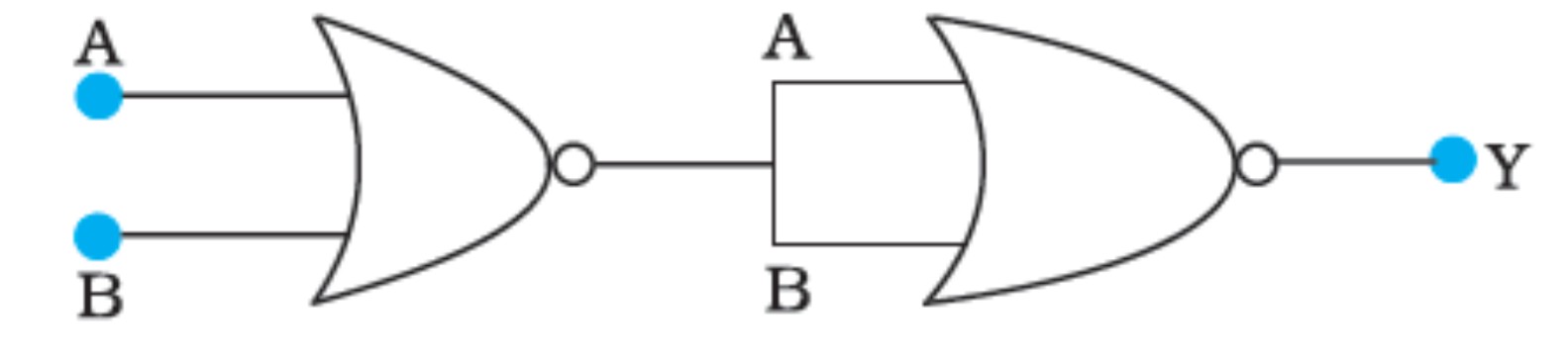
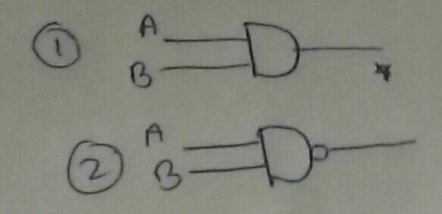
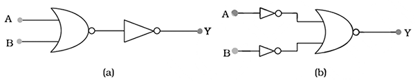
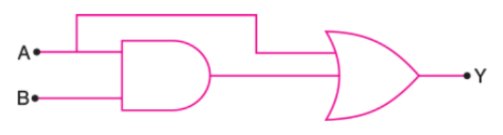
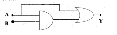
You are given the two circuits as shown in fig . show that circuit (a) acts as OR gate while the circuit (b) act as AND gate.
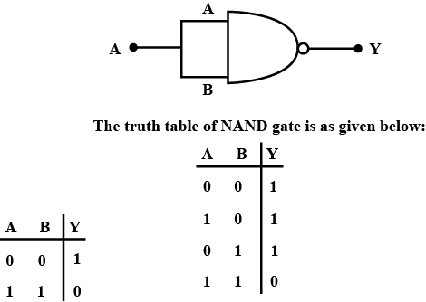
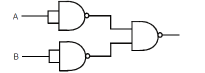
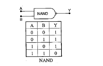
Write the truth table for a NAND gate connected as given in fig.
Hence identify the exact logic operation carried out by this circuit.
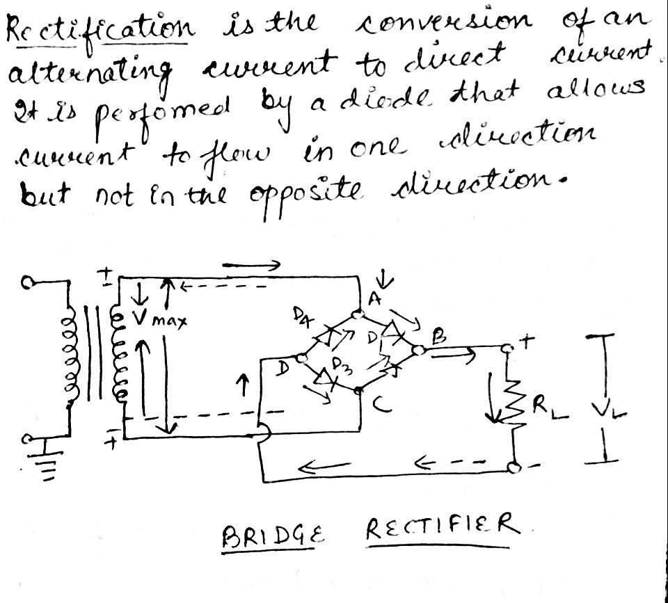
What is rectification? Draw the figure of bridge wave rectifier.
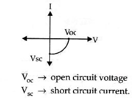
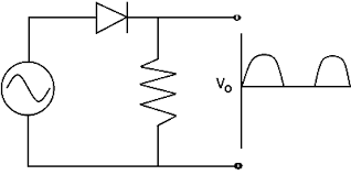
Observe the following figure. Which property of diode is indicated here? Explain that property.
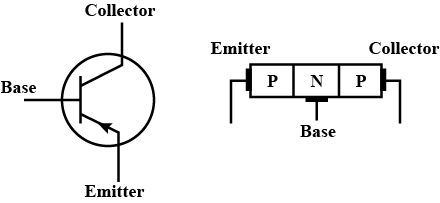
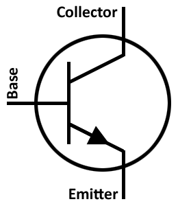
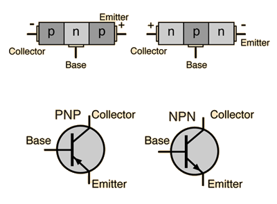
Write the circuit symbol of $$p-n-p$$ transistor.
Write down the name of that logic gate in which the output is 1 when all the inputs are 1.
What do you mean by a logic gate?
In a p-n-p transistor circuit the collector current is $$ 10 mA $$ if $$ 90$$ % of the holes reach the collector , find emitter and base current.
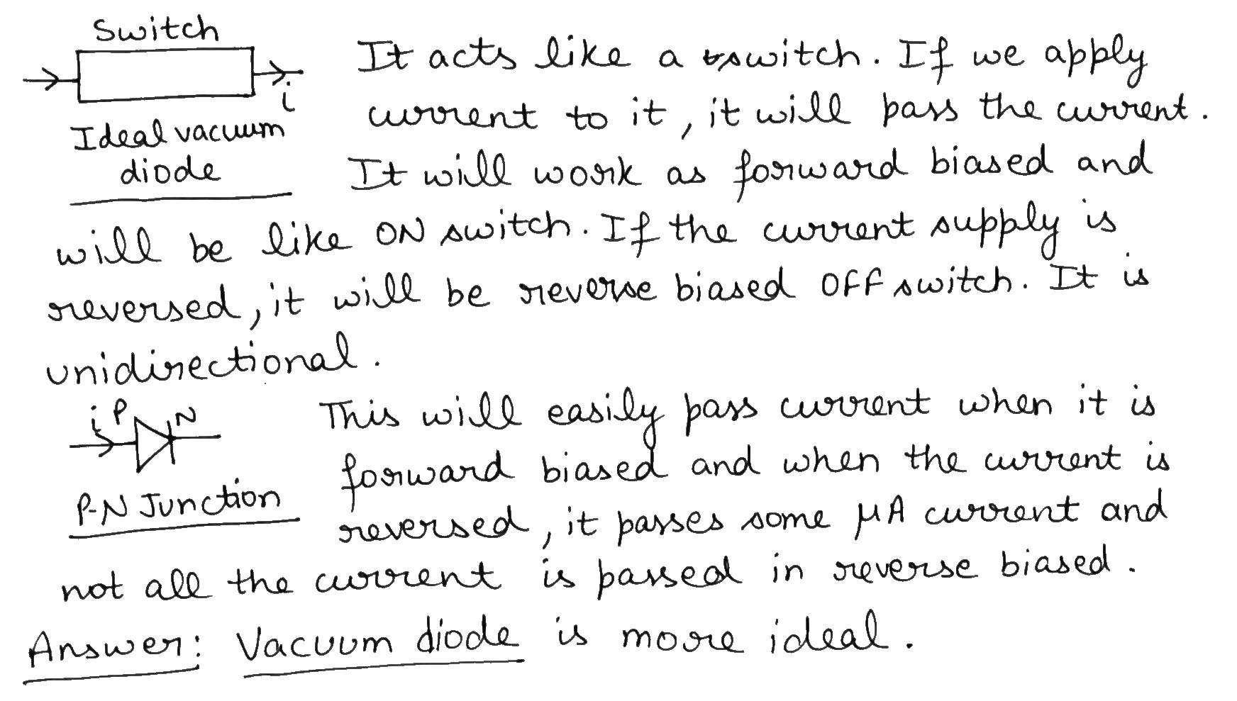
An ideal diode should pass a current freely in one direction and should stop it completely in the opposite direction. Which is closer to ideal-vacuum diode or a p-n junction diode ?
In a full-wave rectifier, the output is taken across a load resistor of $$800$$ ohm. If the resistance of diode in the forward biased condition is $$200$$ ohm, the efficiency of rectification of ac power into dc power is(in percentage)
A certain computer chip that is about the size of a postage stamp $$(2.54 cm ,2.22 cm)$$ contains about $$3.5$$ million transistors. If the transistors are square, what must be their maximum dimension? (Note: Devices other than transistors are also on the chip,and there must be room for the interconnections among the circuit elements. Transistors smaller than $$0.7$$ mm are now commonly and inexpensively fabricated.)
Even though the p-type and n-type semiconductors have holes and electrons respectively as majority charge carries, why are they electrically neutral? Explain.
The source of electric current for a hand held transistor is _____ .
Write any two distinguishing features between conductors, semiconductors and insulators on the basis of energy band diagrams.
Match the following:
Left column lists the level of integration and right column lists the number of circuit components.
Mention important characteristics and applications of a diode.
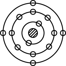
How many electrons are there is the outermost shell of silicon atom?
So the correct answer is $$4$$
What is called a hole?
What is a semi conductor diode or junction diode?
What are conductors and insulators? Give examples.
Suggest any two situations in which photocells can be used as automatic switches.
In semiconductor physics, what is meant by a rectifier?
Silicon nitride has band gap energy of _______________eV.
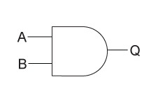
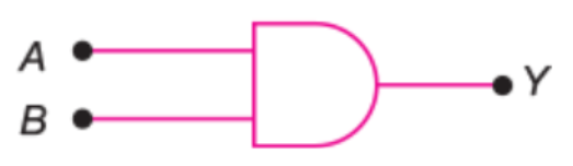
Draw the logic symbol of AND gate.
State the difference between laser light and ordinary light
Draw a block diagram of a simple radio receiver
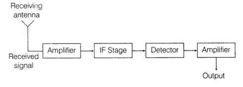
In a radio receiver, the device that separates AF signals from RF signals is ___________.
The more doped region in the transistor is ...........................
Draw the circuit symbol of $$n-p-n$$ transistor.
Zener diode is used as ......................
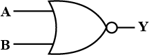
Identify the gate.

Draw the logic symbol of the gate.
Explain why NAND gate is known as universal gate.
What type of gate is this,
Whats the difference between
Carbon, Silicone, and Germanium all have the same number of electrons in an outer most shell. Explain?
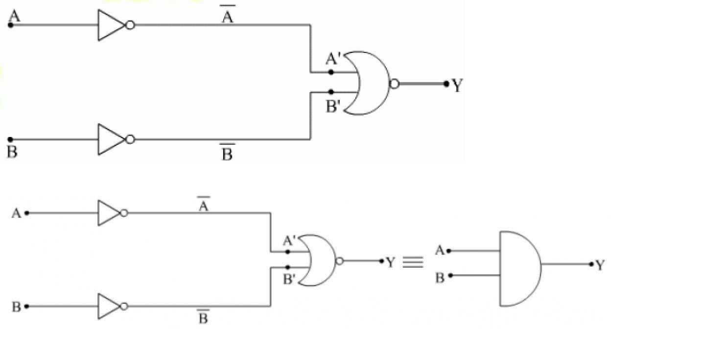
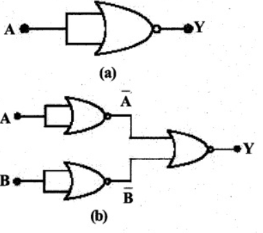
The outputs of two NOT gates are fed to a NOR gate. Draw the logic circuit of the combination of gates. Give its truth table. Identify the gate represented by this combination.
Output from A from NOT gate = $$\bar{A}$$
Output from B from NOT gate = $$\bar{B}$$
Output from NOR gate = $$\bar{\bar{A} + \bar{B}} = A.B $$So, From above we can deduce that, the resultant is a AND gate.
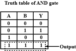
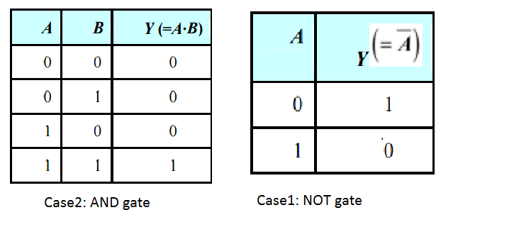
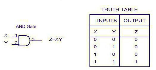
| A | B | Y=AB |
| 0 | 0 | 0 |
| 0 | 1 | 0 |
| 1 | 0 | 0 |
| 1 | 1 | 1 |
In what respect is an LED different from an ordinary PN - junction diode? Where should we prefer LEDs over ordinary incandescent lamps? Why?
What is a transistor? Why is it so called? What are the advantages of transistors over vacuum tubes?
In half-wave rectification, what is the output frequency if the input frequency is $$50\ Hz$$
What is the output frequency of a full-wave rectifier for the same input frequency.
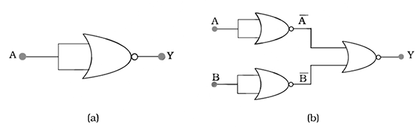
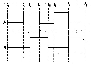
Write the truth table for the circuits given in figure. consisting of NOR gates only. Identify the logic operations (OR, AND, NOT) performed by the two circuits.
You are given the two circuits as shown in Fig. Show that circuit (a) acts as OR gate while the circuit (b) acts as AND gate.
Draw a circuit diagram of n-p-n transistor amplifier in CE configuration. Under what condition does the transistor act as an amplifier?

Transistor should be operated in active region to work as an amplifier.
Emitter-Base junction (i.e. input circuit) should be forward biased.
Collector-Base junction (i.e. output circuit) should be reverse biased.
Write the truth table for the combination of the gates shown. Name the gates used.
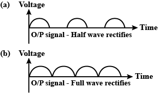
A graph of the output from an A.C. generator is given. This is given as:
(a) an input to a half wave rectifier
(b) an input to a full wave rectifier
Give graphic representations of the outputs in the cases (a) and (b).

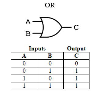
Write the truth table of logic OR gate.
With reference to semiconductor devices, define a p-type semiconductor and a Zener diode. What is the use of a Zener diode?
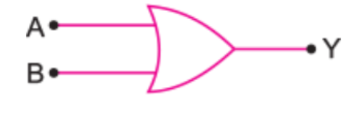
Construct the logic symbol, Boolean expression, circuit diagram and truth table for an OR gate.
Logic Symbol:
Truth Table of $$OR$$ gate
| A | B | Y=A+B(OUTPUT) |
| 0 | 0 | 0 |
| 0 | 1 | 1 |
| 1 | 0 | 1 |
| 1 | 1 | 1 |
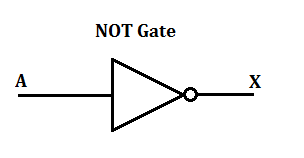
Make logic symbol and write Boolean expression of NOT gate.
Boolean expression of NOT gate is $$X = \bar{A}$$
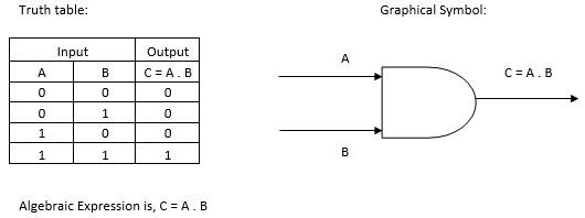
Construct the logic symbol, Boolean expression and truth table for an AND gate.
For a common emitter amplifier. dc(direct current) current gain is $$100$$. If the base current is $$20\mu$$A, calculate the collector and emitter current.
The arrangement given represents a logic gate.
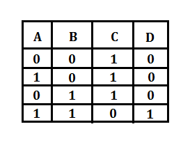
Copy the following truth table and complete it showing outputs at C and D.
| A | B | C | D |
| $$0$$ | $$0$$ | ||
| $$1$$ | $$0$$ | ||
| $$0$$ | $$1$$ | ||
| $$1$$ | $$1$$ |

Hence the truth table for the above circuit is shown here.
Transistors used for making NOT gate.why?
A semiconductor doped with a donor impurity is.
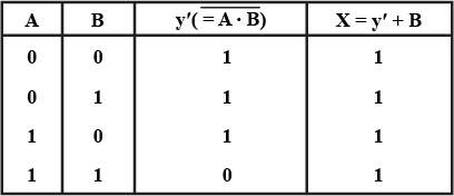
Write down output Y in terms of inputs A and B.
In a zener -regulated power supply a zener diode with $$V_z=6$$ volt is used for regulation. The load current is to be $$4mA$$ and the unregulated input is $$10$$ volt. What should be he value of series resistor $$R_s$$.if the current through diode is five time the load current ?
what is the PN junction diode?
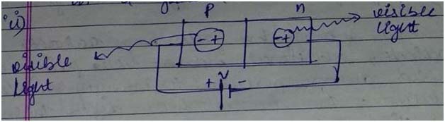
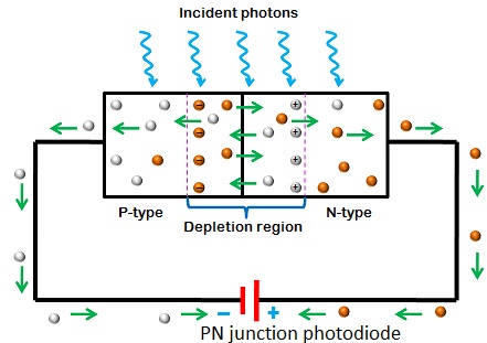
Explain, with the help of a circuit diagram, the working of a photo-diode. Write briefly how it is used to detect the optical signals.
OR
Mention the important considerations required while fabricating a $$p-n$$ junction diode to be used as a Light Emitting Diode (LED). What should be the order of band gap of an LED if it is required to emit light in the visible range?
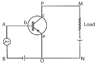
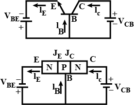
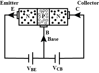
When is a transistor said to be in active state? Draw a circuit diagram of a p-n-p transistor and explain how it works as a transistor amplifier. Write clearly, why in the case of a transistor (i) the base is thin and lightly doped and (ii) the emitter is heavily doped.
- The transistor is said to be in the active state when collector junction is reverse biased and emitter junction is forward biased. A transistor is operated in actual region if it is used as an amplifier.
- A transistor as an amplifier using pnp transistor:

The input signal to be amplified is applied across the input circuit and the amplified output signal obtained across the output circuit having load resistance.
Hence, $$I_{C}=I_{B}+I_{C}$$
The collector voltage $$V_{o}=$$ applied voltage $$V_{CE}$$ - voltage drop across $$R_{L}$$.
i.e. $$V_{o}=V_{CE}-I_{C}R_{L}$$ ...(i)
During the positive half cycle of the input signal, the forward bias of emitter- Base junction decreases. As a result, $$I_{E}$$ and hence $$I_{C}$$ decreases. So, voltage drop across $$R_{L}$$ decreases. According to equation (i), collector or output voltage $$V_{o}$$ increases. Since collector is connected to negative terminal of the battery, so increase in collector voltage implies that collector becomes more negative. Thus, an amplified negative signal is obtained across the output.
During the negative half cycle of the input signal, the forward bias of emitter-base junction increases. As a result, the emitter current $$(I_{E})$$ and hence $$I_{C}$$ increases. Thus voltage drop across $$R_{L}$$ increases and according to equation (i), $$V_{o}$$ decreases. Since collector is connected to negative terminal of the battery, so decrease in collector voltage means that collector becomes less negative. In other words, the amplified positive signal is obtained across the output. - The base is thin and lightly doped
The majority carriers from the emitter region move towards the collector region through the base. If the base is made thick and heavily doped, then most of the majority carriers will combine with the charge carriers in the base while passing through it. Hence, only a small number of majority carriers will reach the collector region. As a result, the output or collector current will be decreased considerably. Therefore, the base region of a transistor is made thin and lightly doped, so that minimum number of majority carriers passing through base get neutralized and large output is available. - The emitter is heavily doped
Because emitter contains the largest amount of charge carriers out of all regions in the transistor. The role of an emitter is to inject a large amount of charge carriers into the base, which then travels onto the collector so that switching or amplification can occur.
(i) Distinguish between a conductor and a semi conductor on the basis of energy band diagram
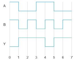
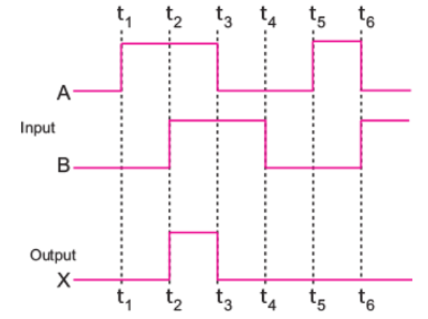
(ii) The following figure shows the input waveforms (A, B) and the output waveform (Y) of a gate. Identify the gate, write its truth table and draw its logic symbol.
Show on a graph, the variation of resistivity with temperature for a typical semiconductor.
$$\rho =\dfrac{m}{ne^{2}\tau }$$
where n = number density of electrons

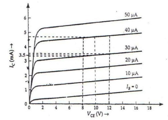
Output characteristics of an $$n-p-n$$ transistor in $$CE$$ configuration is shown in the figure. Determine:
(i) dynamic output resistance
(ii) dc current gain and
(iii) ac current gain at an operating point $${V}_{CE}=10 V$$, when $${I}_{B}=30 \mu A$$.
How is a Zener diode fabricated? What causes the setting up of high electric field even for small reverse bias voltage across the diode?
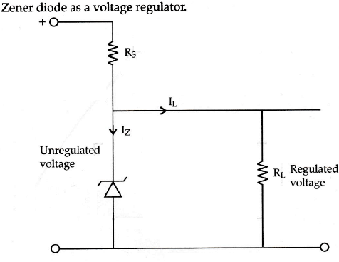
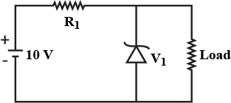
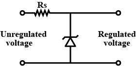
Describe, with the help of a circuit diagram, the working of Zener diode as a voltage regulator.
- Heavily doped p and n junction are to be used for fabricating zener diode.
- The breakdown voltage of the material should be considered to avoid the destruction of the device.
Zener diodes have breakdown voltages ranging from 3-200 Volts. - The zener diodes are fabricated with precise breakdown voltages, by controlling the doping level during manufacturing.
The zener or breakdown voltage depends on the concentration of doping. The n and p regions of zener diode are heavily doped. The depletion layer of heavily doped p-n junction diode is very thin. Since electron field $$\epsilon = -\dfrac{dV}{dr}$$ across the junction would be very high even for small voltage. this electron field is called ionizing field.
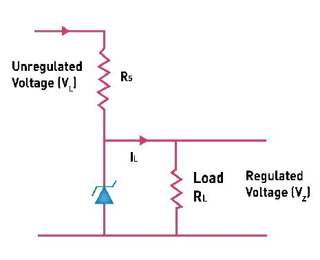
Zener Diode as a Voltage Regulator:
The zener diode is connected across the fluctuating voltage source through a dropping resistor of resistance $$R_{S}$$. The constant voltage supply is obtained across positive Load resistance $$R_{L}$$. When the input voltage increases, resistance of zener diode decreases and hence current through the diode increases to high value.
As a result, a large voltage drop occurs across the dropping resistance $$R_{S}$$. Hence, the output voltage across $$R_{L}$$ is maintained to the desired value. When the input voltage decreases, the current through the diode also decreases. So now small voltage drop takes place across the resistance $$R_{S}$$ and the output voltage across $$R_{L}$$ is maintained at a desired constant value.
Thus, we get a constant voltage in spite of fluctuating input voltage. Hence, zener diode acts as a voltage regulator.
Explain, with the help of a circuit diagram, the working of a p-n junction diode as a half-wave rectifier.
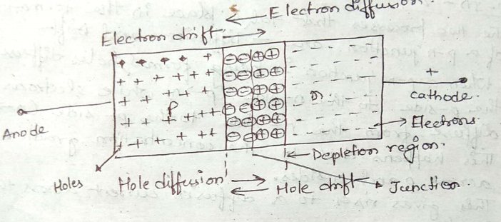
(a) State briefly the processes involved in the formation of p-n junction explaining clearly how the depletion region is formed.
(b) Using the necessary circuit diagram, show how the V-I characteristics of a p-n junction are obtained in
(i) Forward biasing
(ii) Reverse biasing
How are these characteristics made use of in rectification?
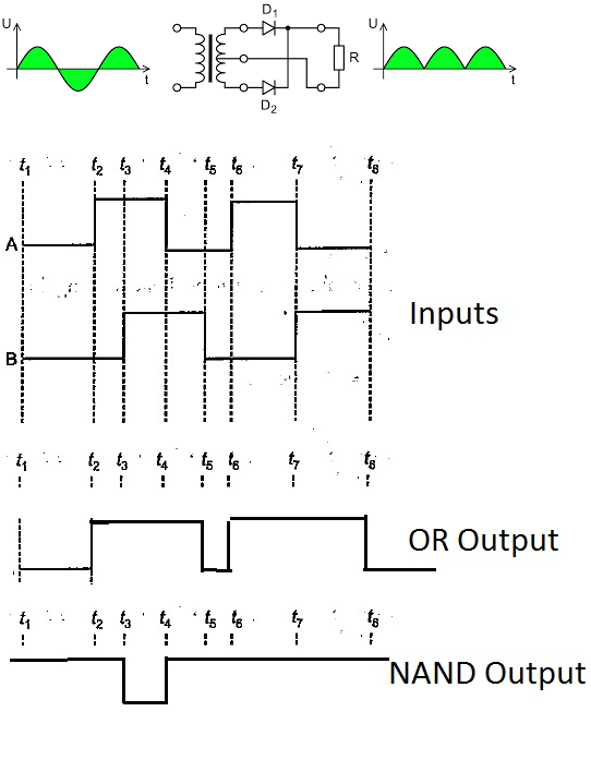
(a) Draw the circuit diagram of a full wave rectifier using $$p-n$$ junction diode.
Explain its working and show the output, input waveforms.
(b) Show the output waveforms (Y) for the following inputs $$A$$ and $$B$$ of
(i) OR gate (ii) NAND gate
(a)
The full wave rectifier circuit consists of two power diodes connected to a single load resistance and each diode taking it in turn to supply current to the load. When a point of the transformer is positive with respect to another point, diode conducts in the forward direction.
When a point of the transformer is positive with respect to another point, then diode conducts in the forward direction and the current flowing through resistor is in the same direction for both half-cycles. As the output voltage across the resistor is the phasor sum of the two wave forms combined, this type of full wave rectifier circuit is also known as a bi-phase circuit.
(b)
(i) OR gate - gives an output of zero when both inputs are zero, else output is 1.
(ii) NAND gate - gives an output of 0 when both inputs are 1, else gives an output of 1.
In the circuit shown in the figure identify the equivalent gate of the circuit and make its truth table .
How does a diode acts as a rectifier.
Give the circuit symbol of a diode.

The arrowhead represents the p-type semiconductor and the vertical bar represents the n-type semiconductor. The arrow represents the direction of conventional electric current through the diode.
Fill in the blanks.
In an npn transistor p type semi conduct is sandwiched between ___________.
What are semiconductors? Give examples.
These are the materials with the forbidden energy gap between valence and conduction band $$< 3 eV$$. It is less than that of insulators $$ (> 3 eV) $$ and more than that of conductors.

Compound semiconductors: Gallium, arsenide, Indium, phosphide, cadmium, sulphide etc.
Mention the applications of a transistor.
Match the items in List 1 with items in list 2
Match the items in List 1 with items in List 2
State one important use of a Zener diode.
Prepare a truth table for the combination of gates shown in figure.

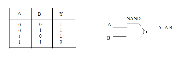
What is NAND gate? Write its truth table.
Write the function of the three segment of a transistor.
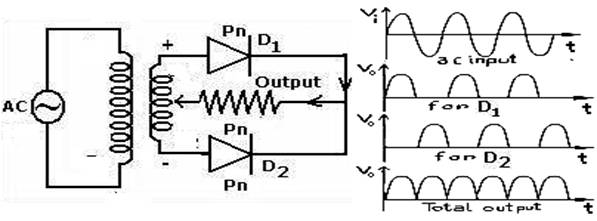
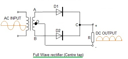
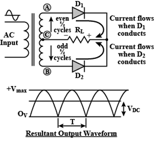
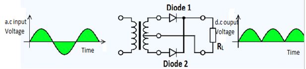
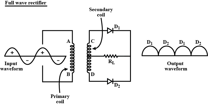
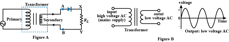
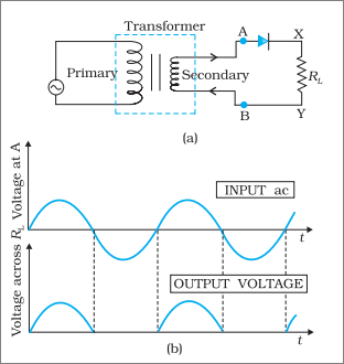
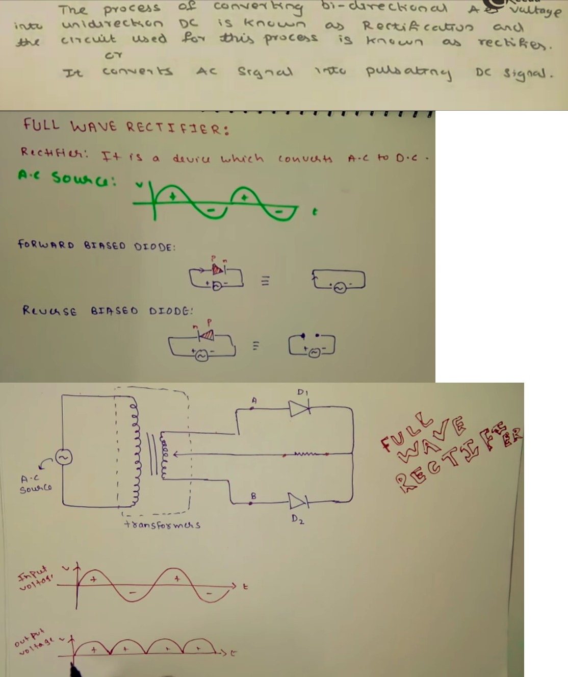
What is rectifier? Explain with neat circuit diagram the action of semiconductor diode as a full wave rectifier.
Action of semiconductor diode as a full wave rectifier:
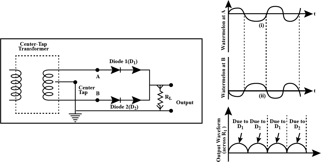
Electric circuit: The alternating voltage to be rectified is applied across primary coil $$(P_1P_2)$$ of a transformer with a centre tapped secondary coil $$(S_1S_2)$$. The terminals $$S_1, S_2$$ of the secondary coil are connected to the two p-regions of two junction diode-$$D_1$$ and $$D_2$$ respectively. The centre tap T is connected to the ground. The load resistance $$R_L$$ is connected across the common n regions and the ground.
Working: During one half cycle of the input, terminal $$S_1$$ of secondary is positive while $$S_2$$ is negative with respect to the ground. During the half cycle, diode $$D_1$$ is forward biased and conducts, while diode $$D_2$$ is reverse biased and does not conduct. The direction of current $$I_L$$ through $$R_L$$ is in the sense shown.
During the next half cycle of the input voltage, $$S_2$$ becomes positive while $$S_1$$ is negative with respect to T Diode. $$D_2$$ now conducts sending a current $$I_L$$ through $$R_L$$ in the same sense as before. $$D_1$$ now does not conduct. Thus, the current through $$R_L$$ flows in the same direction i.e., It is unidirectional, for both halves of the full-wave of the input. This is called full wave rectification.
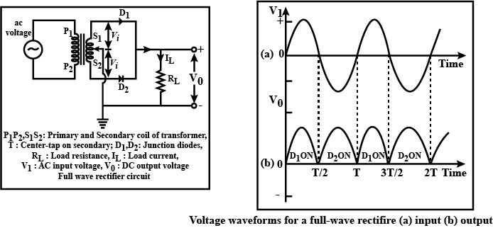
Figure shows the circuit of an electronic device.
(i) Which electronic device: a rectifier, an amplifier or an oscillator does the circuit represent?
(ii) State where the input voltage is applied and where the output voltage is available.
(iii) Compare the output voltage of this circuit with its input voltage.
What are the advantages of Integrated Circuits (IC)
State the properties and uses of a Junction Diode.
State the properties and uses of a Junction transistor.
The Junction Transistor can be used as:
- Current amplifier: The larger collector current $$I_C$$ is proportional to the base current $$I_B$$ according to the relationship $$I_C=\beta I_B$$ , or more precisely it is proportional to the base-emitter voltage $$V_{BE}$$. The smaller base current controls the larger collector current, achieving current amplification.
- Switch: For switching applications transistor is biased to operate in the saturation or cutoff region. Transistor in cutoff region will act as an open switching whereas in saturation will act as a closed switch.
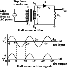
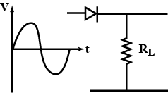
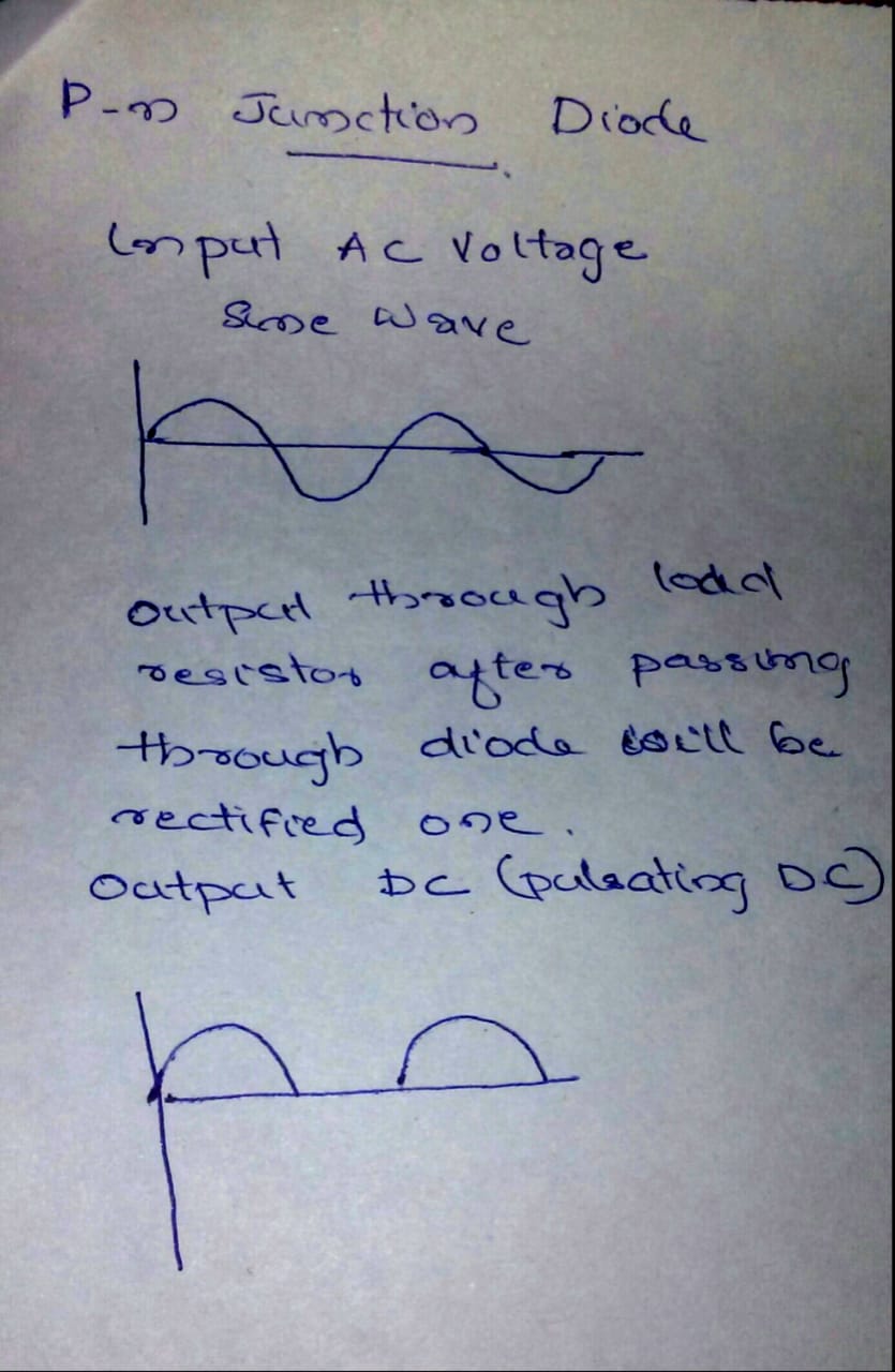
Explain the working of a diode as half wave rectifier.
The figure shows the circuit for half wave rectification. The a.c. voltage $$\left( { V }_{ S } \right)$$ to be rectified is obtained across the secondary ends $${ S }_{ 1 }{ S }_{ 2 }$$ of the transformer. The $$P$$-end of the diode $$D$$ is connected to $${ S }_{ 1 }$$ of the secondary coil of the transformer. The $$N$$-end of the diode is connected to the other end $${ S }_{ 2 }$$ of the secondary coil of the transformer, through a load resistance $${ R }_{ L }$$. The rectified output voltage $${ V }_{ dc }$$ appears across the load resistance $${ R }_{ L }$$.
During the positive half cycle of the input a.c. voltage $${ V }_{ S }$$, $${ S }_{ 1 }$$ will be positive and the diode is forward biased and hence it conducts. Therefore, current flows through the circuit and there is a voltage drop across $${ R }_{ L }$$. This gives the output voltage.
During the negative half cycle of the input a.c. voltage $$\left( { V }_{ S } \right)$$, $${ S }_{ 1 }$$ will be negative and the diode $$D$$ is reverse biased. Hence, the diode does not conduct. No current flows through the circuit and the voltage drop across $${ R }_{ L }$$ will be zero. Hence, no output voltage is obtained. Thus corresponding to an alternating input signal, unidirectional pulsating output is obtained.
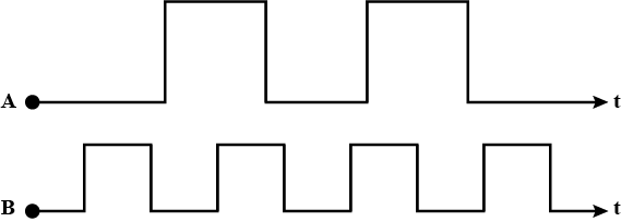
Show the output waveform of OR gate for the following input waveforms of $$A$$ and $$B$$
What is extrinsic semiconductor? How many types of these are? Write their names. Explain the processes which are occurred during the formation of a P-N junction. Determine the electric field produced at a P-N junction when width of depletion layer is $$1$$ micrometer and barrier potential is $$0.7$$ volt.
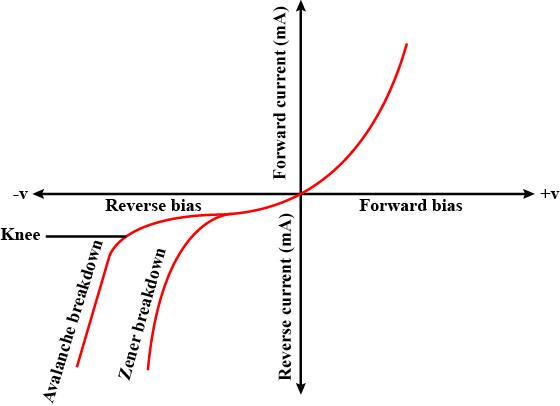
Distinguish between Avalanche breakdown and Zener breakdown.
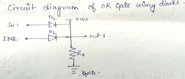
Draw the circuit diagram of AND gate using diodes.
What is rectification? Explain the working of a fullwave rectifier. Draw necessary circuit diagram.
When point B is positive (in the negative half of the cycle) with respect to point C, diode $$D_2$$ conducts in the forward direction and the current flowing through resistor $$R$$ is in the same direction for both half-cycles.
As the spaces between each half-wave developed by each diode is now being filled in by the other diode the average DC output voltage across the load resistor is now double that of the single half-wave rectifier circuit and is about $$0.637V_{max}$$, assuming no losses.
What is rectification? With relevant circuit diagram and waveforms explain the working of a P-N junction diode as a full-wave rectifier.
Answer the following question :
(i) Write the functions of the three segments of a transistor.
(ii) The figure shows the input wave forms A and B for 'AND' gate . Draw the output wave form and write the truth table for this logic gate.
Truth table
| Input | Output | |
| A | B | Y = A.B |
| $$ 0 $$ | $$ 0 $$ | $$ 0 $$ |
| $$ 0 $$ | $$ 1 $$ | $$ 0 $$ |
| $$ 1 $$ | $$ 0 $$ | $$ 0 $$ |
| $$ 1 $$ | $$ 1 $$ | $$ 1 $$ |
Explain avalanche breakdown in a diode and zener breakdown in a zener diode.
(a) In the following diagram, which bulb out of $$B_1$$ and $$B_2$$ will glow and why?
(b) Draw a diagram of an illuminated p-n junction solar cell.
(c) Explain briefly the three processes due to which generation of emf takes place in a solar cell.
What is rectification? Explain the working of a full wave rectifier.
What is a Fermi energy level? What is its position in case of an intrinsic semiconductor?
What is rectification? Explain the working of a full-wave rectifier with a diagram. What is a zener diode? How will a zener diode be connected in a circuit generally?
Working:-
Here the configuration used to rectify is of centre tap type and the concept used is that diodes operates only in forward biased, that is, in reverse biased a diode is switched off.
The input waveform is AC, that is, it changes its polarity periodically. In the first half cycle, the diode D1 is in forward biased and is On so it behaves as a short circuit where as the diode D2 is in reverse biased and is Off so it behaves as as an open circuit. The current in the circuit follows the path A-D1-C-R-O-A.
In the second half cycle of the i/p waveform, the polarities change and the diode D1 is in reverse biased and is Off thus behaving as an open circuit where as the diode D2 is in forward biased and is On thus behaving as a short circuit. The current in the circuit follows the path B-D2-C-R-O-B.
The direction of current through the load resistor R does not change that is it flows in downward direction in both the cycles.
Zener diode- It is a diode made up of highly doped p-n junctions which allows the current to flow through it even in reverse biased mode unlike other diodes.
A zener diode is generally connected in reverse biased mode in a circuit for controlling purposes.
Draw the diagram of a Helium-Neon laser tube and label the parts.
Write the logic symbols and prepare the truth tables of the following gates.
(i) AND
(ii) NOR.
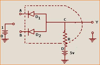
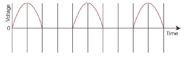
A diode is connected to the output of a transformer as shown in the figure given below. Analyse the figure.
a) Draw a time-voltage graph for the current obtained across AB.
b) What is the function of the diode in the circuit?
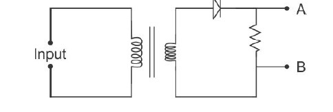
b) The diode functions as a rectifier in the circuit. It allows only the positive voltage cycle to flow through the circuit and blocks the negative cycle.
(A) What do you mean by barrier potential of diode?
(B) With help of a diagram explain the working of a full wave rectifier.
B) Full wave rectifier:
A full rectifier is an arrangement of four or more diodes in a bridge circuit configuration which provides the same output polarity for either input polarity. It is used for converting an alternating current (AC) input into a direct current (DC) output.
For half cycle of input AC, one diode out of the two, will get forward biased and will conduct, while the other diode, being reverse biased, will not conduct. For other cycle of input signal, the diode, which was reverse biased, will get forward biased and will conduct, and the other diode will get reverse biased and will stop conducting. Hence we obtain a unidirectional output voltage for the positive as well as for negative half cycles.
Distinguish between conductor and semiconductor on the basis of band theory of solids.
What is main logic gates? How many types are they? Draw their symbols and Truth Table.
Mainly logic gate are of three types. OR, AND & NOT gate.
(i) OR Gate:
Truth Table:
| Input | Output | |
| $$A$$ $$0$$ $$0$$ $$1$$ $$1$$ | $$B$$ $$0$$ $$1$$ $$0$$ $$1$$ | $$Y=A+B$$ $$0$$ $$1$$ $$1$$ $$1$$ |
Truth Table:
| Input | Output | |
| $$A$$ $$0$$ $$0$$ $$1$$ $$1$$ | $$B$$ $$0$$ $$1$$ $$0$$ $$1$$ | $$Y=A \cdot B$$ $$0$$ $$0$$ $$0$$ $$1$$ |
Truth Table:
| Input $$A$$ | Output $$Y=\bar { A } $$ |
| $$0$$ $$1$$ | $$1$$ $$0$$ |
What is an intrinsic semi conductor? Give two examples.
Write the name of device $$'X'$$ in the following given diagram. Explain its working making its circuit diagram.
What is a transistor? Mention any two uses of transistor.
What is logic gates? Write two names of universal logic gates.
Explain working of half wave rectifier using $$p-n$$ junction diode with the help of circuit diagram.

When the positive half of a.c input signal flows through the primary coil, as induced emf is set up in the secondary coil due to mutual induction. The direction of induced emf is such that the upper end of secondary coil becomes positive and lower end becomes negative. Since upper end of secondary coil is connected to n-region of the junction diode, so the junction diode is forward biased during the positive half of input a.c. Thus, the junction diode conducts and flow of current starts in the direction shown by arrows. The output voltage which varies in accordance with input half cycle is obtained across $$R_{L}$$.

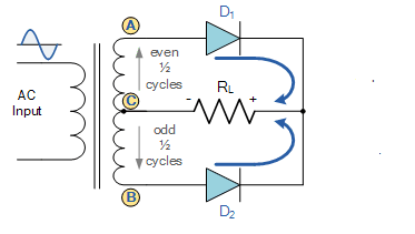
Draw the circuit diagram of full-wave rectifier using two p-n junction diodes and explain its working. Show the input and output waveforms.

The a.c input signal is fed to the primary (P) coil of the transformer. The p-region of both the diodes $$D_{1}$$ and $$D_{2}$$ are connected to two ends of secondary coil (S). The load resistance $$(R_{L})$$ across which output voltage is obtained is connected between common point of n-regions of diodes and central topping of the secondary coil.
When positive half cycle of input a.c signal flows through the primary coil, induced emf is set up in the secondary coil due to mutual induction. The direction of induced emf is such that the upper end of secondary coil becomes positive while lower end becomes negative. Thus, $$D_{1}$$ diode is forward biased and $$D_{2}$$ is reverse biased. So, current through $$D_{1}$$ flows through circuit in a direction shown.
During negative half cycle of input a.c signal, diode $$D_{1}$$ is reverse biased and $$D_{2}$$ is forward biased. The current due to $$D_{2}$$ flows through circuit in a direction shown.
Since, both the halves of input a.c (wave) are rectified, so the junction diode is called Full-wave rectifier.

Construct the circuit symbol of Zener diode.

How is $$p-n$$ junction diode used as a half-wave rectifier?
Explain its working, draw a neat circuit diagram. Show the waveforms of input and output voltages.
Working:
The a.c input signal to be rectified is fed to the primary (P) coil of the transformer. The secondary (S) coil is connected to the junction diode through a load resistance $$R_{L}$$.

When the positive half of a.c input signal flows through the primary coil, as induced emf is set up in the secondary coil due to mutual induction. The direction of induced emf is such that the upper end of secondary coil becomes positive and lower end becomes negative. Since upper end of secondary coil is connected to p-region of the junction diode, so the junction diode is forward biased during the positive half of input a.c. Thus, the junction diode conducts and flow of current starts in the direction shown by arrows. The output voltage which varies in accordance with input half cycle is obtained across $$R_{L}$$.
When negative half cycle of a.c input flows through the primary coil, again induced emf is set up across the secondary coil due to mutual induction. Now the direction of induced emf is such that upper end of the secondary coil becomes negative and lower end becomes positive. So the junction diode is reverse biased. Hence the junction diode does not conduct, and therefore, we get no output across load resistance during negative half of input a.c. The input and corresponding output voltages as shown:
Write the two processes that take place in the formation of a $$p-n$$ junction. Explain with the help of a diagram, the formation of depletion region and barrier potential in a $$p-n$$ junction.
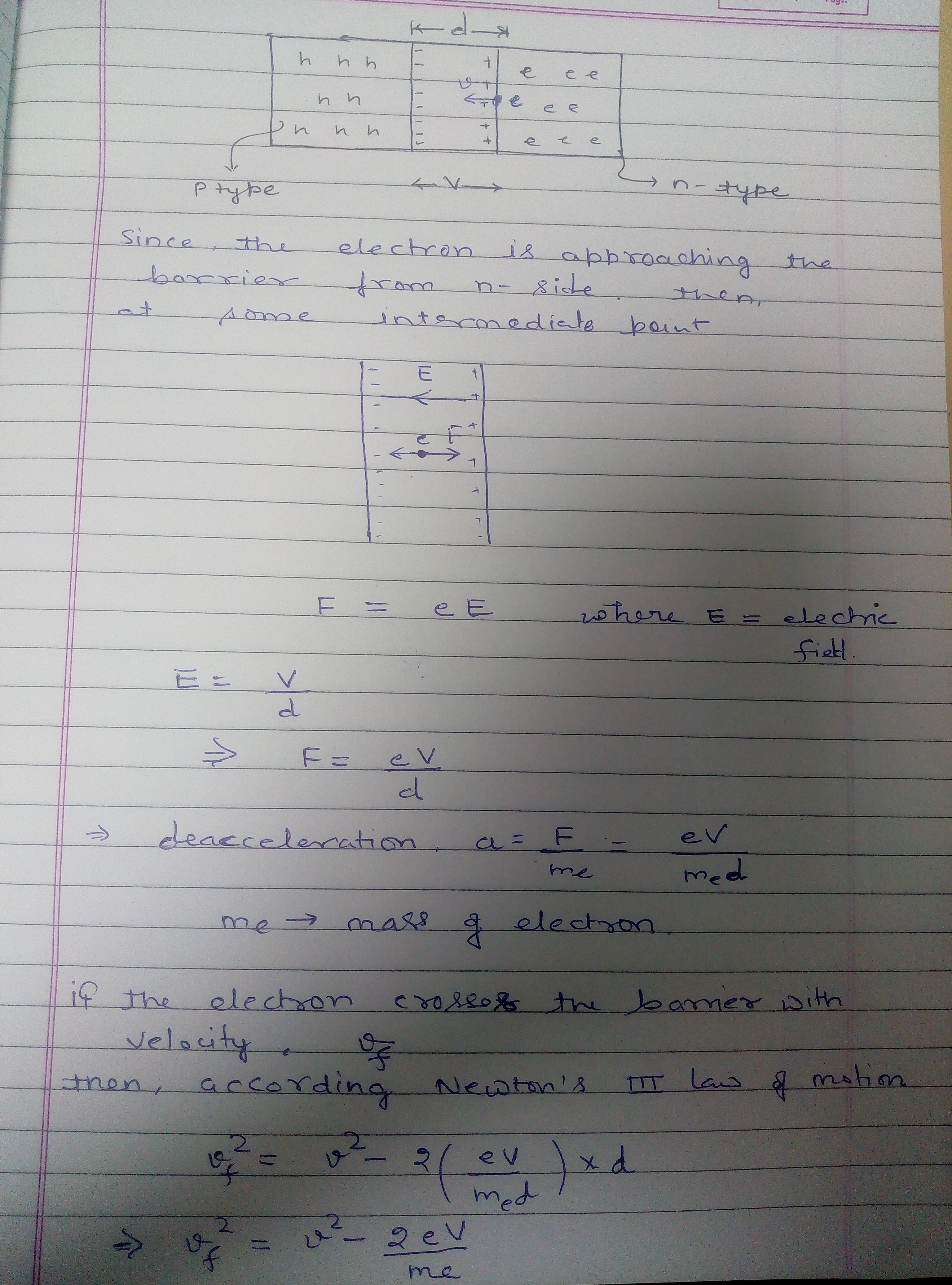
A potential barrier V volts exists across a P-N junction. The thickness of the depletion region is 'd'. An electron with velocity 'v' approaches P-N junction from N-side. Find the velocity of the electron crossing the junction.
Why is the base region of the transistor thinly doped?
The input resistance of a transistor is $$1000\Omega$$. On changing the base current by $$10\mu A$$, the collector current increases by $$2mA$$. If a load resistance of $$5\ k\Omega$$ is used in the circuit, calculate (i) the current gain, (ii) voltage gain of the amplifier.
What is a rectifier? With a suitable circuit diagram, describe the action of a full wave rectifier by drawing input and output waveforms.
During negative half cycle appearing at $$A$$, the diode $${D}_{1}$$ is reverse biased. End $$B$$ is positive and diode $${D}_{2}$$ is forward biased. The diode $${D}_{2}$$ conducts. A current flow through $${R}_{L}$$ in the same direction and output voltage appears across $${R}_{L}$$
What are n-type and p-type semiconductor?
Draw circuit diagram of common base configuration.
Explain the importance of the PIV rating of a diode.
In the forward bias arrangement of a PN-jucnction diode.
The electric resistance of depletion layer is large bacause
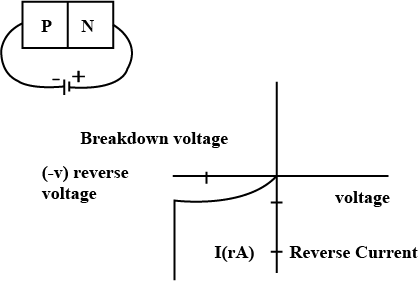
Draw diagram for a P-N junction to obtain reverse bias characteristic curves. Explain the phenomenon of reverse breakdown for a P-N junction in reserve bias state by following processes-
(i) Avalanche breakdown
(ii) Zener breakdown
When we increase the reverse voltage the depletion layer breaks at certain reverse voltage this voltage is known as break down voltage.
The break down of depletion layer can be two type.
(1) Avalanche breakdown : the minority charge carrier get highly accelerated. The kinetic energy becomes high enough at they knock-off electrons from the covalent bonds of semiconductors. The newly generated electron holes pairs also accelerated and cause ionisation the depletion layer & break down the depletion layer.
(2) Zener breakdown : Due to high doping in zener diode the depletion layer has small width. When large reverse biased applied across such a diode, the depletion layer & the energy bands get modified, As the depletion width is very small, small voltage will set high electric field of $$4 \times 10^7 V/m$$. this high electric field strips off many electrons from valence band which tunnel to the n-side through the this depletion layer. It gives rise to a large reverse current or breakdown current this breakdown in a diode due to the band to band tunneling is called zener breakdown.
Write the important considerations which are to be taken into account while fabricating a p-n junction diode to be used as a Light Emitting Diode (LED) . What should be the order of band gap of an LED, if it is required to emit light, in the visible range? Draw a circuit diagram and explain it action.
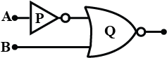
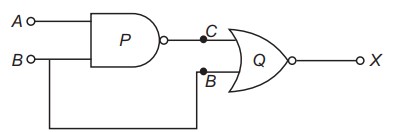
(i) Write the truth tables of the logic gates marked $$P$$ and $$Q$$ in the given circuit.
(ii) Write the truth table for the circuit.
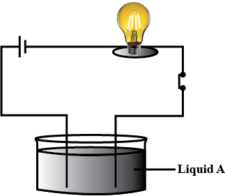
Reashma set up an experiment using liquid 'A' in the beaker as shown in the figure. She observed that the bulb glows. Then she replaced the liquid 'A' by another liquid 'B', this time the bulb did not glow. Rani suggested replacing the bulb by an LED. They observer that the LED glows. Give reason.
Draw the circuit arrangement for studying the $$V_I$$ characteristics of a p-n junction diode in reserve bias. Plot the $$V-I$$ characteristics in this case.
The potential difference across the collector is a transistor, used in common emitter mode is $$1.5 V$$, with the collector resistance of $$3 k\Omega$$. Find $$(i)$$ the emitter and $$(ii)$$ the base current, if the $$d.c$$ gain of the transistor is $$50$$.
Identify the logic gates marked $$'P'$$ and $$'Q'$$ in the given circuit. Write the truth table for the combination.

Truth table for the combination:
How many minimum NAND GATEs are required for obtaining an output of $$A.B+C.D$$?

Answer the following :
(i) Write the truth table of the following gate.
(ii) What will be the values of inputs A and B for the Boolean expression
$$ ( A \bar{+} B) . ( \bar {A.B}) = 1 $$
What is a rectifier? With the help of a neat circuit diagram explain the working of a full wave rectifier.
The electrical conductivity of a semiconductor increases when electromagnetic radiation of wavelength shorter than $$248\ nm$$ is incident on it. The forbidden band energy for the semiconductor in $$eV$$ is
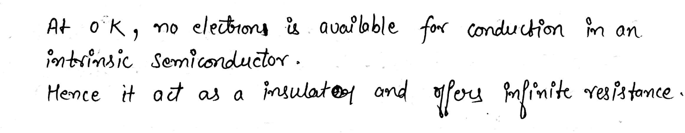
What is the resistance of an intrinsic semiconductor at OK ?
Can we measure the potential difference across an unbiased p-n junction by connecting a sensitive voltmeter across it ?
Name fundamental logic gates.
Name two semiconductor materials.
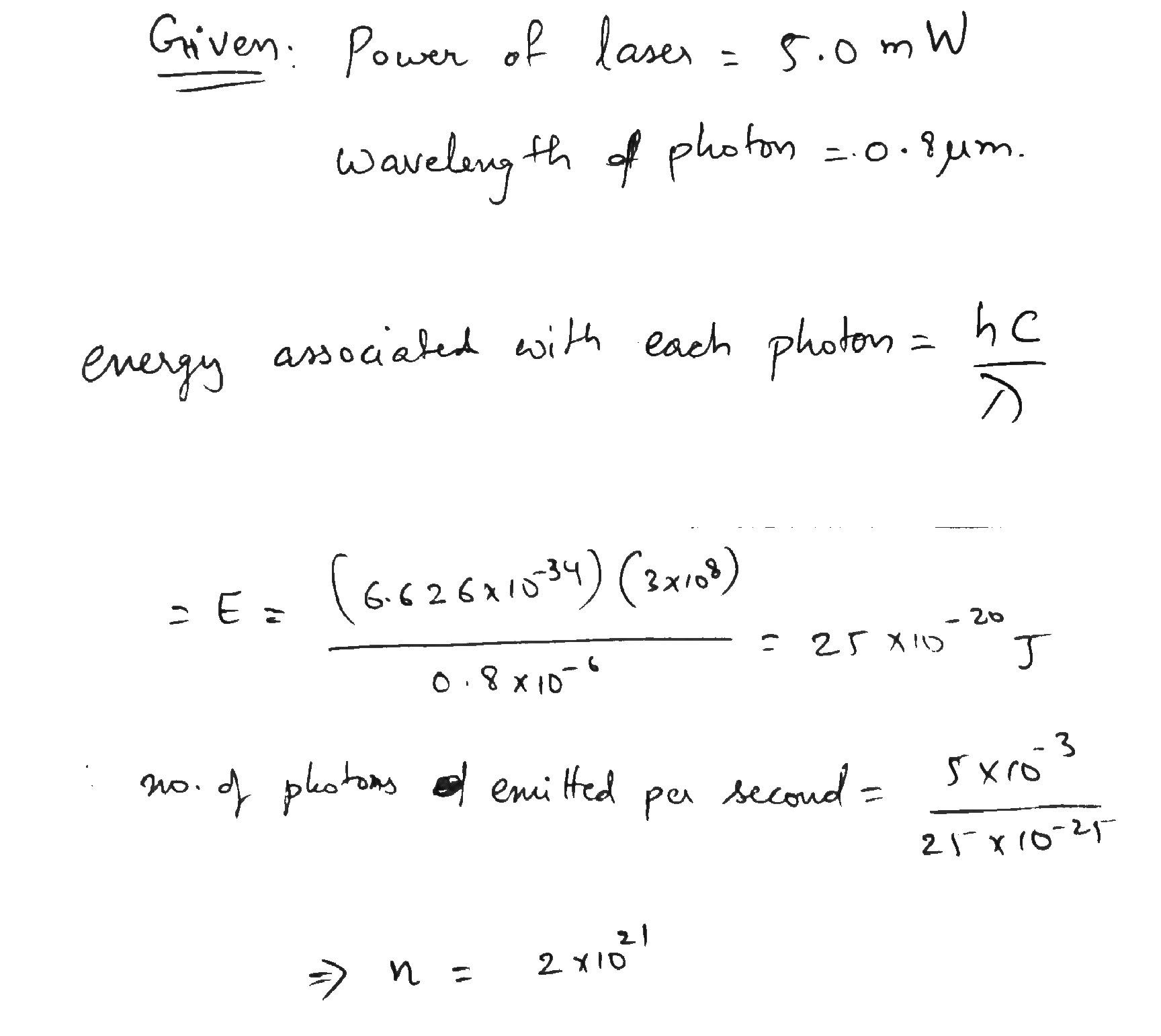
The active volume of a laser constructed of the semi-conductor GaAlAs is only $$ 200 \mu
m^3$$ (smaller than a grain of sand), and yet the laser can continuously deliver 5.0 mW of power at a wavelength of $$0.80\mu m$$. At what rate does it generate photons?
In a transistor , doping level in base is increased slightly. How will it affect base current ?
At what temperature would an intrinsic semiconductor behave like a perfect insulator ?
Name the logic gate marked P and Q in the given logic circuit .
In a transistor , doping level in base is increased slightly. How will it affect collector current ?
Draw the output waveform at X , using the given inputs A , B for the logic circuit shown alongside . Also identify the gate.
Name the logic gate whose repetitive use can make digital circuits .
What signal voltage is represented for positive logic state $$ 1$$ ?
(a) Explain briefly the process of emission of light by a Light Emitting diode. (LED).
(b) Which semiconductor are preferred to make LEDs and why ?
(c) Give two advantages of using LEDs over conventional incandescent lamps.
The output of an OR gate is connected to both the inputs of a NAND gate. Draw the logic circuit of this combination of gates and write its truth table.
Name the logic gate which can be realised by using p-n junction diode in the given diagram. Give its logic symbol and write the truth table. Name the gate which will be obtained by combining with a NOT gate.
How is a light emitting diode fabricated ? Briefly state is working. Write any two important advantages of LEDs over the conventional incandescent low power lamps.
Distinguish between a metal and an insulator on the basis of energy band diagrams.
In a common emitter mode of a transistor , the d.c current gain is $$ 20 $$ , the emitter is $$ 7 \, mA $$. Calculate (i) base current and (ii) collector current.
Explain the following :
LEDs are made of compound semiconductor and not by elemental semiconductors.
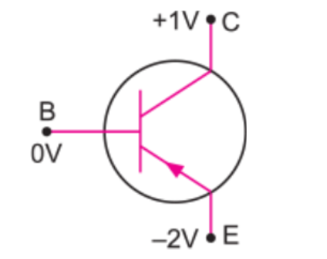
In the figure given alongside is, (i) the emitter and (ii) the collector forward or reverse biased ? With the help of a circuit diagram explain the action of npn transistor.
Answer the following questions :
(i) What is an 'Integrated circuit (I.C)' ? Distinguish between (i) linear I.C and (ii) Digital I.C.
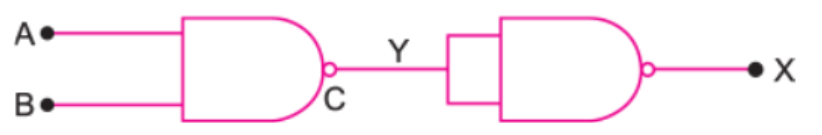
(ii) Identify the equivalent gate for the following circuit and write its truth table.
The inputs A and B are inverted by using two NOT gates and their outputs are fed to the NOR gate as shown above .
Analyse the action of the gate (1) and (2) and identify the logic gate of the complete circuit so obtained. Give its symbol and truth table.
Output of gate $$ (2) , Y_2 = B \bar{+} B = \bar{B} $$
Output $$ Y = Y_1 \bar{+} Y_2 = \bar{A} \bar{+} \bar{B} = \bar{\bar{A}} . \bar{\bar{B}} = AB $$
Thus gates (1) and (2) act on 'NOT' gates and the complete circuit acts as 'AND' gate . The symbol and truth table of complete circuit are given below :
Truth table
| $$ A $$ | $$ B $$ | $$ Y $$ |
| $$ 0 $$ | $$ 0 $$ | $$ 0 $$ |
| $$ 1$$ | $$ 0 $$ | $$ 0 $$ |
| $$ 0 $$ | $$ 1 $$ | $$ 1 $$ |
| $$ 1 $$ | $$ 1 $$ | $$ 1 $$ |
Explain the forward and the reverse characteristic of a Zener diode.
Write the truth table for the circuits given in fig. consisting of NOR gates only. identify the logic operation (OR, AND , NOT) performed by the two circuits.
Draw the circuit diagram of a half-wave rectifier. Explain its working. What is the frequency of ripple in its output?
What do you mean by a truth table?
Why is the base of a transistor made thin and is lightly doped?
Express by a truth table, the output Y for all possible inputs $$ A $$ and $$ B $$ in the logic as shown
How is a Zener diode different than an ordinary diode?
What is rectification? Draw the circuit diagram of half wave rectifier and explain its working. Show the input ac voltage and output voltage waveforms from the rectifier circuit.
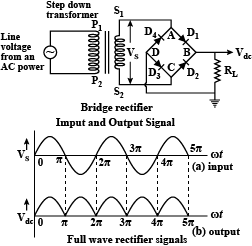
What is rectification? Explain the working of bridge rectifier. Draw the input and output signals.
Working of a Bridge rectifier :
A bridge rectifier is shown in figure. There are four diodes $$D_{1}, D_{2}, D_{3}$$ and $$D_{4}$$ used in the circuit, which are connected to form a network. The input ends $$A$$ and $$C$$ of the network are connected to the secondary ends $$S_{1}$$ and $$S_{2}$$ of the transformer. The output ends $$B$$ and $$D$$ are connected to the load resistance $$R_{L}$$.
During positive input half cycle of the arc voltage, the point $$A$$ is positive with respect to $$C$$. The diodes $$D_{1}$$ and $$D_{3}$$ are forward biased and conduct, whereas the diodes $$D_{2}$$ and $$D_{4}$$ are reverse biased and do not conduct.
Hence, current flows along $$S_{1}ABCDS_{2}$$ through $$RL$$. During negative half cycle, the point $$C$$ is positive with respect to $$A$$. The diodes $$D_{2}$$ and $$D_{4}$$ are forward biased and conduct, whereas the diodes $$D_{1}$$ and $$D_{3}$$ are reverse biased and they do not conduct. Hence, current flows along $$S_{2}CBADS_{1}$$ through $$R_{L}$$. The same process is repeated for subsequent half cycles. It can be seen that current flows through $$R_{L}$$ in the same direction, during both half cycles of the input a.c. signals. The output signal corresponding to the input signal is shown in figure. The efficiency of the bridge rectifier is approximately $$81.2$$%.
Advantages of bridge rectifier : (i) Centre tap on the secondary of the transformer is not necessary, (ii) Smaller transformer can be used and (iii) It is suited for high voltage applications.
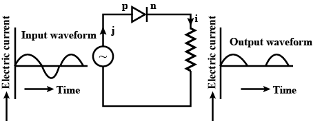
If in a $$p-n$$ junction diode, a sinusoidal input signal is applied as shown.
Then, the output signal across $$R_{L}$$ will be:
the intrinsic semiconductor at room temperature is
Suppose a pure Si crystal has $$5\times 10^{28}$$ atoms per $$m^3$$. It is doped by $$1$$ ppm concentration of pentavalent As. Calculate the number of electrons and holes. Given that $$n_i=1.5\times 10^{16}$$ per $$m^3$$.
Write the truth table of AND gate.
What is rectifier? Explain the working of p-n junction diode as a full-wave rectifier with the help of suitable circuit diagram.
Draw a circuit diagram of an n-p-n transistor with its emitter-base junction foward biased and base-collector junction reverse biased.
Briefly describe its working.
Explain how a transistor in active states exhibits a low resistance at its emitter-base junction and high resistance at its base-collector junction.
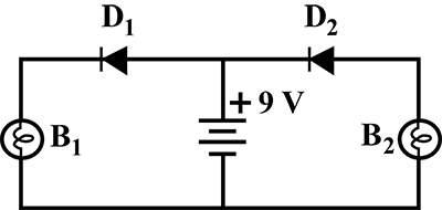
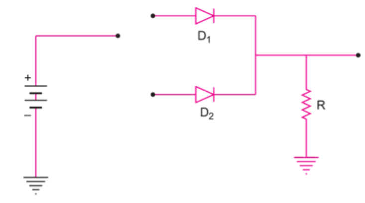
If each diode in figure, has a forward bias resistance of $$125\Omega$$ and infinite resistance in reverse bais, what will be the values of the current $${I}_{1},{I}_{2},{I}_{3}$$ and $${I}_{4}$$?
A Zener of power rating $$1W$$ is to be used as a voltage regulator. If Zener has a breakdown of $$5V$$ and it has to regulate voltage which fluctuated between $$3V$$ and $$7V$$, what should be the value of $${R}_{s}$$ for safe operation (Figure)?
The current amplification is 0.99 for any transistor in the common-base configuration. Calculate the change in collector current when there is a 5.0 milliampere change in emitter current. What will be the change in base current?
A transistor is connected in common emitter configuration. A power supply of $$ 8 \vee $$ is there in the collector circuit and the potential drop of $$ 0.5 \mathrm{V} $$ is on the resistance of 80012 connected in series with the collector. If current amplification factor is $$ a=0.96 . $$ Then calculate the base current.
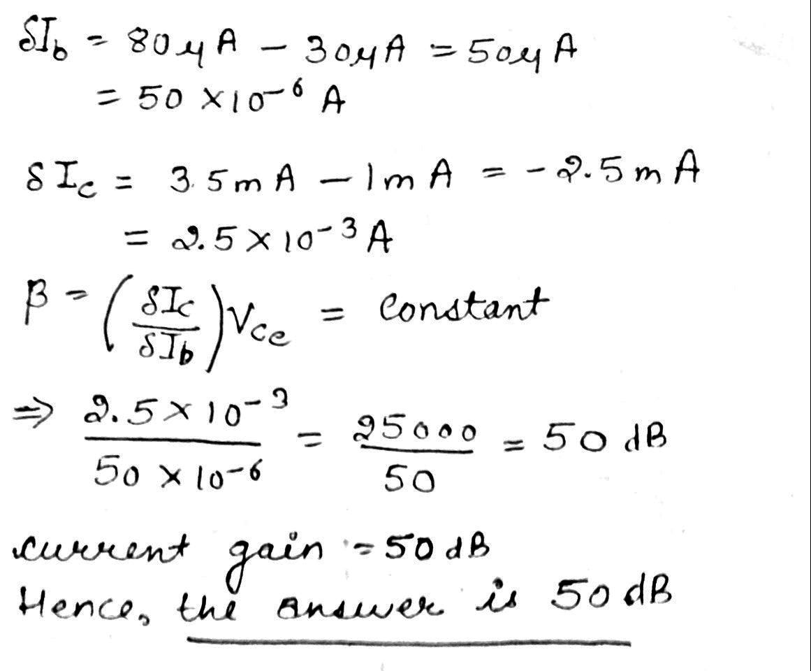
When the base current in a transistor is changed from $$30 \, \mu\, A$$ to $$80 \mu \,A$$, the collector current is changed from $$1.0 \mu \,A$$ to $$3\cdot 5\, \mu \,A$$. Find the current gain $$\beta$$
A silicon-based MOSFET has a square gate $$0.50$$ mm on edge. The insulating silicon oxide layer that separates the gate from the $$p-type$$ substrate is $$0.20$$ mm thick and has a dielectric constant of $$4.5.$$ $$(a)$$ What is the equivalent gate – substrate capacitance (treating the gate as one plate and the substrate as the other plate)? $$(b)$$ Approximately how many elementary charges e appear in the gate when there is a gate–source potential difference of $$1.0 V?$$
What is the direction of diffusion current in junction diode?
Class 12 Medical Physics Extra Questions
- Alternating Current Extra Questions
- Atoms Extra Questions
- Current Electricity Extra Questions
- Dual Nature Of Radiation And Matter Extra Questions
- Electric Charges And Fields Extra Questions
- Electromagnetic Induction Extra Questions
- Electromagnetic Waves Extra Questions
- Electrostatic Potential And Capacitance Extra Questions
- Magnetism And Matter Extra Questions
- Moving Charges And Magnetism Extra Questions
- Nuclei Extra Questions
- Ray Optics And Optical Instruments Extra Questions
- Semiconductor Electronics: Materials, Devices And Simple Circuits Extra Questions
- Wave Optics Extra Questions